الإلكترونيات الاستهلاكية، والإلكترونيات السيارات، وأنظمة التحكم الصناعي والطاقة الجديدة الثلاثية (البطارية والمحرك ووحدة التحكم)، تشهد حاجة غير مسبوقة لـ"مقاومة الرطوبة، ومقاومة رذاذ الملح، ومقاومة التآكل، ومقاومة التسرب الكهربائي". تُبنى الطبقات الوقائية التشكيلية التقليدية (conformal coating) في الغالب على الأكريليك، والبولي يوريثان، والمطاط السيليكوني، والباريلين، بسماكة تتراوح غالبًا بين 25–75 ميكرومتر، وتغطي بشكل شامل لكنها تؤثر على تشتت الحرارة، وتزيد الوزن، وتصعب إصلاحها. أما طلاء الحماية النانوي (يُسمى غالبًا "الطلاء النانوي" "طلاء النانو ثلاثي الحماية") فيوفر غشاءً شفافًا بسماكة 1–10 ميكرومتر أو حتى دون الميكرومتر، وبفضل الخصائص المائية النافرة، والعزل الكهربائي المنخفض، والقدرة على الطلاء الانتقائي، أصبح خيارًا جديدًا للحماية الإلكترونية الدقيقة. يستعرض هذا المقال من أربعة جوانب: آلية الفشل، وإحداثيات المعايير، والتشكيل النانوي، والفحص والاختيار، مع ربط المؤشرات الكمية بمعايير حقيقية مثل IPC وIEC وGB، دون اختلاق أرقام.
كيسين للمواد الجديدة (kexinMaterials) توفر في مجال الطلاء النانوي الوظيفي والحماية الإلكترونية الثلاثية حلولًا أكريليكية، وبولي يوريثان، وتعديل نانوي مائي النفور، وسيتناول هذا المقال أيضًا المعلمات النموذجية للحماية النانوية على مستوى PCB من بياناتها التقنية العامة، لمساعدة القراء على بناء حكم اختيار "قائم على المعايير".
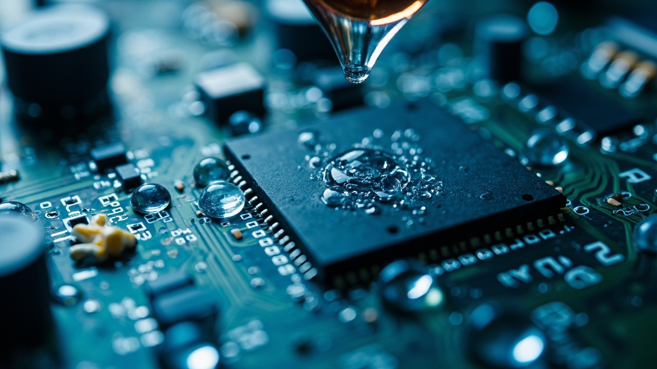
أولاً: لماذا يحتاج الجهاز الإلكتروني إلى حماية: ثلاثة أنواع من الفشل
ينشأ فشل الأنظمة الإلكترونية في الغالب من الإجهاد البيئي:
- الرطوبة الحارة والتكاثف: تشكل جزيئات الماء على سطح PCB غشاءً سائلاً متصلًا، مما يخفض مقاومة العزل السطحي (SIR)، ويحفز التيار المتسرب والهجرة الكهروكيميائية (ECM، نمو التفرعات القصيرة).
- رذاذ الملح والتآكل: في المعدات الساحلية والمركبات والأجهزة الخارجية، ي corrodes أيون Cl⁻ نقاط اللحام وإطارات الأطراف، خاصة لحامات خالية من الرصاص (SAC) الأكثر حساسية.
- غبار موصل وقوس كهربائي: الغبار الموصل الدقيق + الرطوبة = التسرب السطحي والقوس، خاصة في المكونات عالية الجهد.
هدف طبقة الحماية هو، ضمن قيود "العزل الكهربائي، وتشتت الحرارة، والقابلية للإصلاح"، حجب الماء/الملح/الغبار بأقصى حد. وهذا يختلف عن الحماية المضادة للتآكل الثقيلة العادية: طبقة الإلكترونيات أرفع، وتتطلب عزلًا كهربائيًا منخفضًا، ولا تحجب الإشارة، وتُطبق انتقائيًا.
1.1 الهجرة الكهروكيميائية (ECM): مسار التقصير الأكثر خفاءً
ECM هو الفشل الأكثر إثارة للحذر في الطلاء الإلكتروني: تحت الجهد الانحيازي + الرطوبة، تذوب أيونات المعدن (خاصة الفضة والنحاس والقصدير) من الأنود، وتهاجر على طول الغشاء المائي السطحي وتترسب مختزلة على الكاثود على شكل تفرعات شجرية (dendrite)، مما يربط في النهاية بين الموصلات المجاورة مسببًا قصرًا. يتطلب حدوثها ثلاثة عناصر معًا: ① وجود أيونات معدنية قابلة للذوبان وفرق جهد انحيازي؛ ② وجود غشاء مائي متصل على السطح (توفره الرطوبة العالية/التكاثف)؛ ③ تلوث أيوني يوفر الإلكتروليت. الوقاية تعتمد على ثلاث خطوط دفاع: إزالة التلوث الأيوني (IPC-TM-650 2.3.25)، وحجب الغشاء المائي (نافر مائي/تشكيلي)، ورفع مقاومة العزل السطحي SIR (عزل المادة). وهذا يفسر لماذا "النظر فقط إلى تدحرج قطرة الماء" غير كافٍ—فـ ECM فشل تآزري للأيونات والحقل الكهربائي والماء، وغياب أي عنصر يصعب حدوثه، بينما في الميدان تتوفر العناصر الثلاثة غالبًا معًا.
1.2 التكاثف: حالة تشغيل حقيقية أكثر شيوعًا من "الغمر في الماء"
معظم فشل الإلكترونيات ليس بغمر الجهاز بالكامل، بل بتكوين تكاثف عندما يتجاوز الفارق اليومي أو التشغيلي نقطة الندى. يفرش التكاثف غشاءً مائيًا متصلًا على سطح PCB، وهو سبب مباشر لانخفاض SIR وحدوث ECM. هناك فكرتان لمنع التكاثف: الأولى خفض احتمال تكوين الغشاء بعد وصول السطح لنقطة الندى (الغشاء النافر يجعل الماء على شكل حبات لا غشاء، ويتدحرج بسهولة ليأخذ الغبار)؛ والثانية الحفاظ على عزل عالٍ حتى لو تكون الغشاء (مقاومة جوهرية عالية للمادة + تحكم بالتلوث الأيوني). وهذا يوضح أن قيمة "الغشاء النانوي لمقاومة الرش/التكاثف" هي الأكبر في معظم السيناريوهات المدنية والمركبات غير المغمورة—فهو يستهدف بالضبط أنماط الفشل الأكثر تكرارًا، لا الغمر المتطرف.
ثانيًا: إحداثيات المعايير: IPC وIEC وGB
لطلاء التشكيل الإلكتروني منظومة معايير ناضجة:
- IPC-CC-830 "طلاء تشكيلي للوحات المطبوعة": يحدد مستويات الأداء والاختبارات للطلاء التشكيلي (العزل، مقاومة الحرارة، مقاومة الرطوبة، رذاذ الملح، مثبط اللهب، إلخ)، وهو المعيار الفعلي لصناعة الإلكترونيات في أمريكا الشمالية؛ وIPC-SP-980 وغيرها من الأدلة تكمل العملية.
- IEC 61086 "طلاء تشكيلي لعزل كهربائي": معيار اللجنة الكهروتقنية الدولية، يصنف الأنواع والمتطلبات، ويكمل IPC.
- GB/T ذات الصلة: يشير المحلي غالبًا إلى IPC/IEC بالمكافأة أو المواصفات الصناعية (مثل متطلبات طلاء الحماية الثلاثية للتجميع الإلكتروني).
2.1 إصدارات المعايير والاعتماد المكافئ
عند اختيار المعيار، يجب ملاحظة "علاقة الاعتماد": الحماية الثلاثية الإلكترونية المحلية تعتمد غالبًا مكافئًا لـ IPC/IEC (مثل مواصفات الصناعة GB/T ذات الصلة تُصاغ بالإشارة إلى IPC-CC-830 وIEC 61086)، لكنها ليست دائمًا مطابقة 100% (اختلافات IDT/MOD/NEQ تؤثر على بنود فردية). للمنتجات المصدرة يُنصح بالإشارة المباشرة لرقم إصدار IPC/IEC وسنته (مثل الإصدار الحالي IPC-CC-830)، لتجنب تشكيك العملاء في المصدر عند "الاعتماد على المعيار الوطني". أما درجة حماية IP فـ IEC 60529 وGB/T 4208 متطابقان أساسًا، ويمكن استخدامهما كمرجع لهدف حماية الجهاز الكامل.
- درجة حماية IP (IEC 60529 / GB/T 4208): IPx7 (غمر مائي 1 متر لمدة 30 دقيقة)، IP6X (مقاومة الغبار)، إلخ، هي أهداف حماية للجهاز النهائي، والطلاء النانوي غالبًا وسيلة مساعدة لتحقيق IP لا الوسيلة الوحيدة.
يجب التمييز: الطلاء التشكيلي هو "غشاء عازل تغطية شاملة" (يُتحقق وفق IPC-CC-830)، بينما الطلاء النانوي المائي النافر هو في الغالب "غشاء نافر انتقائي رفيع جدًا" (يُتحقق وفق زاوية التماس وSIR ورذاذ الملح)، ومفهوما الحماية مختلفان، ويُستخدمان غالبًا معًا.
ثالثًا: التشكيل والآلية للطلاء النانوي للحماية
للحماية النانوية الإلكترونية مسارات تقنية رئيسية:
1. غشاء نانوي مائي النفور/فائق النفور: ببناء طاقة سطحية منخفضة + خشونة نانو-ميكروية على سطح PCB باستخدام سلائف فلورية/سيليكانية (مشابهة لـ sol-gel السيراميك السيارات)، لجعل زاوية تماس الماء > 100°–120°، وتتدحرج القطرات مانحة الغبار. الميزة: رفيع جدًا (دون الميكرومتر–عدة ميكرومترات)، لا يؤثر بشكل ملحوظ على تشتت الحرارة والمظهر، يمكن غمر/رش اللوحة بالكامل؛ العيب: مقاومة التآكل والحجب طويل الأمد أضعف من الطبقة التشكيلية السميكة، وهو من مستوى "مقاومة التكاثف/الرش" لا "الغمر الكامل".
2. أكريليك/بولي يوريثان معدل نانويًا: إدخال SiO₂ نانوي/سيراميك نانوي في راتنج الطلاء التشكيلي الكلاسيكي، لرفع الصلابة، ومقاومة التآكل، والعزل الكهربائي، والحرارة، مع الحفاظ على سماكة عشرات الميكرومترات، وسلوك التحقق وفق IPC-CC-830.
3. ترسيب غازي للباريلين (بولي بارا زايلين): رغم أنه ليس تعديلًا بـ"جسيمات نانوية"، لكنه غشاء جزيئي متجانس (عدة ميكرومترات)، يترسب بالبخار عند درجة حرارة الغرفة عبر CVD، بتغطية بلا زوايا ميتة، وعزل منخفض، وتوافق بيولوجي. يُتحقق وفق IPC-CC-830 وMIL-I-46058C (عسكري تاريخي)، وهو الخيار الأول للإلكترونيات عالية الجودة، لكن المعدات غالية وصعب الإصلاح.
بخصوص الأساس الفيزيائي لزاوية التماس والنفور المائي، يمكن الرجوع للمقال المصاحف نفورية الترطيب وزاوية التماس للطلاء النانوي؛ وبخصوص النانو الثلاثي للإلكترونيات، يمكن الرجوع لعنقود الطاقة الجديدة طلاء النانو للحماية الإلكترونية الثلاثية.
3.1 النفور المائي ليس "زاوية واحدة": زاوية التماس، والتأخر، وزاوية التدحرج
عند تقييم الغشاء النانوي النافر، الإبلاغ وحده عن "زاوية تماس 110°" غير كامل. هندسيًا ننظر لأقل من ثلاثة: زاوية التماس الساكنة θ (زاوية قطرة الماء مع سطح الغشاء، >90° نافر، >150° وزاوية تدحرج <10° يعد فائق النفور)؛ تأخر زاوية التماس (فرق الزاوية الأمامية والخلفية، كلما صغر قل بقاء الغشاء المائي المتبقي، وزادت القدرة على "التنظيف الذاتي" لحمل الغبار)؛ زاوية التدحرج (ميل السطح لبدء تدحرج القطرة، كلما صغر سهل انفصال القطرة عند التكاثف). طريقة الاختبار وفق GB/T 30693 (زاوية التماس لرقائق ومواد بلاستيكية السطح)، وISO 19403 (قابلية الترطيب السطحية الصلبة)، ويجب ذكر حجم القطرة، وسائل الاختبار، ودرجة الحرارة والرطوبة والطريقة، وإلا لا يمكن المقارنة. ويجب التنبيه أن زاوية النفور العالية لا تعني موثوقية إلكترونية—فهي فقط مؤشر "إبطاء تكوين الغشاء المائي"، وحد الموثوقية الحقيقية يبقى SIR ورذاذ الملح.
3.2 عتبة الترسيب الغازي للباريلين
يترسب الباريلين عبر تحلل حراري للمركب الثنائي في حجرة مفرغة إلى بخار أحادي، ثم بوليمرة على سطح الركيزة بدرجة حرارة الغرفة، متجانس جزيئيًا، بلا زوايا ميتة، وعزل منخفض. لكن العتبة واضحة: استثمار معدات عالٍ، وبطء معدل الترسيب، وحساسية لحمل الحجرة، والإصلاح يتطلب بلازما أو إزالة بمذيب. لذا يُستخدم في سيناريوهات "الموثوقية تغلب التكلفة" (الطبي المزروع، العسكري، الفضاء، المستشعرات عالية الجودة)، بينما الإلكترونيات الاستهلاكية بكميات كبيرة تميل لتركيبة "نانو نافر + تشكيلي سميك موضعي" لتوازن التكلفة والقابلية للإصلاح.
رابعًا: الفحص الرئيسي: تحويل "الحماية" إلى كمي
| بند الفحص | المعيار الشائع | الوصف |
|---|---|---|
| مقاومة العزل السطحي SIR | IPC-TM-650 2.6.3 / IEC 60326 | القيمة بعد الرطوبة الحارة، لمنع التسرب/الهجرة |
| أداء الطلاء التشكيلي | IPC-CC-830 / IEC 61086 | مقاومة الحرارة، الرطوبة، رذاذ الملح، مثبط اللهب الشامل |
| رذاذ الملح | GB/T 1771 / ASTM B117 | تقييم مقاومة تآكل نقاط اللحام/الأطراف |
| زاوية التماس النافر | GB/T 30693 / ISO 19403 | شدة النفور المائي للغشاء النانوي |
| درجة IP | IEC 60529 / GB/T 4208 | هدف حماية الجهاز من الغمر/الغبار |
| العزل الكهربائي/الجهد | IPC-TM-650 2.5.7 | مقاومة العزل، جهد الانهيار |
وفق بيانات عامة، يمكن لطلاء PCB نانوي نافر مؤهل رفع زاوية تماس الماء فوق 110°، والحفاظ على قيمة SIR عالية بعد دورات رطوبة حارة؛ لكن تحقيق "قابل للغمر" (IPx7/x8) يتطلب عادةً اقتران بختم هيكلي أو طبقة تشكيلية سميكة. عند الشراء يجب التمييز بوضوح بين مستويي حماية "مقاومة الرش/التكاثف" و"قابل للغمر".
4.1 يجب الاتفاق على "تساوي الظروف" قبل الفحص
بيانات SIR ورذاذ الملح من مختبرات مختلفة لا تُقارن مباشرة، المفتاح في محاذاة ظروف الاختبار: ملف درجة الحرارة والرطوبة (40℃/90% أم 85℃/85%)، قيمة الجهد الانحيازي وطريقة التطبيق، سائل الاختبار وعتبة الحكم، والمعالجة المسبقة للعينة (غسل اللوحة أم لا). SIR لنفس الطلاء عند "85℃/85% RH، 100 V، 500 h" أشد بكثير من "40℃/90%، 10 V، 168 h". عند مقارنة بيانات الموردين، يجب المطالبة بظروف اختبار كاملة لا مجرد قيمة مقاومة؛ وعند الضرورة إرسال لطرف ثالث لإعادة الاختبار بإجراء موحد، لإصدار حكم متكافئ.
4.2 كيف تقرأ اختبار رذاذ الملح دون خداع
رذاذ الملح (GB/T 1771 / ASTM B117) ينقسم لن Neutral (NSS)، وحمض الخل (AASS)، ورذاذ الخل المعجل بالنحاس (CASS)، بصرامة متزايدة. عند قراءة التقرير انظر: تركيز المحلول (عادة 5% NaCl)، pH، الحرارة (مستوى 35℃)، المدة، هل العينة مطلية أو مقطوعة، والحكم هل "تآكل مظهر" أم "ت衰减 SIR + مقطع نقطة اللحام". النظر فقط لـ"كم ساعة بلا صدأ أحمر" غير كافٍ—الإلكترونيات تهتم أكثر ببقاء SIR ضمن المعيار بعد الرذاذ، وعدم تكون التفرعات. الادعاء بـ"رذاذ ملح 1000 h" يجب أن يرفق ببيانات SIR وحالة العينة، وإلا بلا حجة.
خامسًا: التطبيق النموذجي وعملية التطبيق
يؤكد تطبيق الحماية النانوية الإلكترونية على "النظافة + الانتقائية":
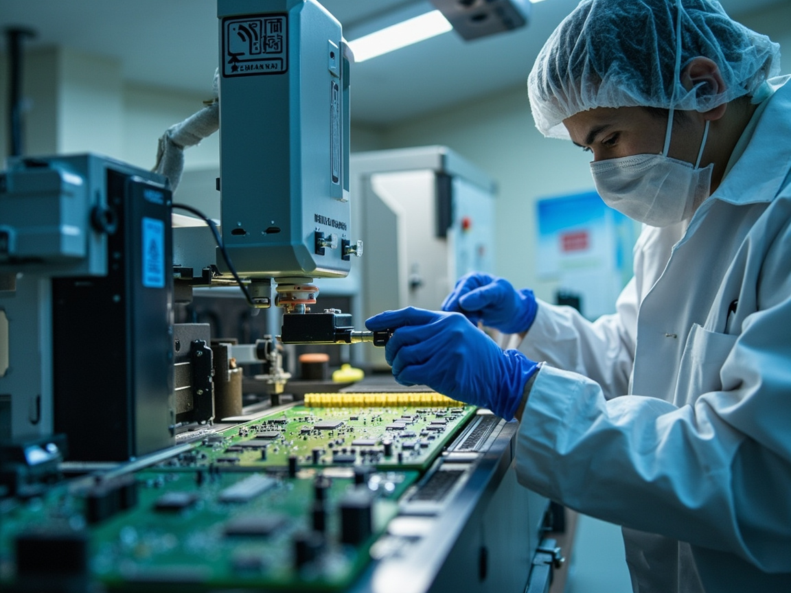
- المعالجة المسبقة: غسل اللوحة بالموجات فوق الصوتية لإزالة بقايا معجون اللحام (يجب أن يصل التلوث الأيوني للمعيار، وفق اختبار التلوث الأيوني IPC-TM-650 2.3.25)، ثم التجفيف.
- التظليل: الموصلات، وأصابع الذهب، وفتحات الصوت، وفتحات المستشعر غالبًا تحتاج تظليل أو فتح لاحق، لتجنب الطلاء الخاطئ مسببًا سوء التوصيل.
- الطلاء: الغمر، الرش، الرش الانتقائي (jet)، الترسيب الغازي، حسب الدقة والإنتاج.
- التركيب: UV، أو حراري، أو درجة حرارة الغرفة، حسب النظام.
- الفحص: المظهر، زاوية التماس، SIR، ورذاذ الملح عند الضرورة.
على عكس الطلاء الصناعي "رملي Sa 2½"، جوهر المعالجة المسبقة الإلكترونية هو "إزالة التلوث الأيوني + التحكم بالرطوبة"، من مقياس ميكرومتري إلى جزيئي. بخصوص التطبيق النانوي العام (رش/غمر/غازي/CVD)، يمكن الرجوع للمقال المصاحف عملية تطبيق الطلاء النانوي.
5.1 طريقة الطلاء والتحكم بالسماكة
تختلف سماكة وتجانس طرق الطلاء اختلافًا كبيرًا: الغمر يعتمد سرعة السحب (علاقة Landau-Levich تقارب السماكة بجذر سرعة السحب)، وسهل التقطر فيحتاج ضبط اللزوجة؛ الرش يعتمد ضغط الذرورة والمسار، مناسب للوحات الكبيرة؛ الـ jet الانتقائي يعتمد مسار CAD، بأعلى دقة لكن استثمار معدات كبير؛ الترسيب الغازي (parylene) يعتمد تركيز البخار الأحادي وتجانس الحجرة، بلا زوايا ميتة لكن صعب الإصلاح. أياً كانت الطريقة، يجب أخذ عينات سماكة بالمقياس الرطب/الجاف (ISO 2808 / GB/T 13452.2)—فالرفيع جدًا يحمي أقل، والسميك جدًا يؤثر على تشتت الحرارة ويولد إجهادًا داخليًا.

سادسًا: نانو نافر مقابل Parylene مقابل تشكيلي تقليدي: مقارنة واختيار
| البعد | تشكيلي تقليدي (أكريليك/PU/سيليكون) | غشاء نانوي نافر | غازي Parylene |
|---|---|---|---|
| السماكة | 25–75 ميكرومتر | دون الميكرومتر–عدة ميكرومتر | عدة ميكرومتر |
| مستوى الحماية | عالٍ (قابل للغمر) | متوسط (مقاومة الرش/التكاثف) | عالٍ (تغطية بلا زوايا ميتة) |
| تأثير تشتت الحرارة | كبير | ضئيل جدًا | صغير |
| القابلية للإصلاح | متوسط (قابل للإذابة) | جيد (سهل إعادة الطلاء) | رديء (يحتاج إزالة) |
| تكلفة المعدات | منخفضة | منخفضة–متوسطة | عالية |
| التحقق المعياري | IPC-CC-830 | زاوية التماس/SIR/رذاذ الملح | IPC-CC-830/MIL |
مبدأ الاختيار: للمتطلب الغمر وعالي الموثوقية (عسكري، طبي، قلب مركبة)، اختر Parylene أو تشكيلي سميك؛ للمتطلب خفيف الوزن، وحساس لتشتت الحرارة، وسهل الإصلاح (إلكترونيات استهلاكية، قابلة للارتداء)، اختر نانو نافر؛ ويمكن دمجهما—نانو نافر أساسًا ثم تشكيلي سميك موضعي للمناطق الحرجة.
6.1 عملية الدمج "نانو أساس + تشكيلي سميك موضعي"
للوحات التي تريد رفيعًا وتشتت حرارة جيدًا، مع موثوقية عالية للمناطق الحرجة، يُستخدم الدمج: أولًا نانو نافر أساس للوحة كاملة (مقاومة الرطوبة، خفض مخاطر الأيونات المتبقية)، ثم تشكيلي سميك انتقائي (أكريليك/PU) لجذور الموصلات، ونقاط لحام التيار العالي، والحواف مناطق الفشل. هكذا نحافظ على تشتت الحرارة والإصلاح الكلي، ونرفع حماية أضعف نقطة. مفتاح الدمج هو توافق الواجهة—يجب التحقق من التصاق النانو والسميك لتجنب الانفصال؛ وتظليل SOP يجب أن يغطي الطبقتين لمنع الطلاء الخاطئ.
سابعًا: مخاطر هندسية ومفاهيم خاطئة
المفهوم الخاطئ الأول: "الغشاء النانوي يمكنه استبدال التشكيلي تمامًا". خطأ. النانو النافر غالبًا لمستوى الرش، والغمر الكامل يعتمد طبقة سميكة أو ختم هيكلي. الثاني: "الأسمك أكثر أمانًا". خطأ. التشكيلي السميك يؤثر على الحرارة، ويسهل تشقق الإجهاد، ويحجب الإشارة. الثالث: "الطلاء دون غسل اللوحة". خطأ. بقايا الأيونات محبوسة تحت الغشاء، وتحت الرطوبة الحارة تسرع ECM. الرابع: "كل الفتحات قابلة للطلاء". خطأ. فتحات الصوت والموصلات تحتاج تظليل انتقائي وإلا فشل الوظيفة.
7.1 مفهومان خاطئان شائعان آخران
الخامس: "SIR مرة واحدة ناجح يعني موثوقية دائمة". خطأ. SIR نتيجة دفعة وظروف معينة، والاتساق الكمي يعتمد التحكم العملية (غسل، معلمات طلاء، مواد واردة)، ويجب أخذ عينات دفعة وضبط إحصائي. السادس: "زاوية النفور أعلى تعني حماية أكثر". خطأ. الغشاء فائق النفور (>150°) إن ضعف الميكانيكي، يفقد بالاحتكاك أثناء التجميع، تاركًا نقاطًا محبة للماء كنقطة بداية ECM؛ السيناريو الإلكتروني يهتم أكثر بـ"تجانس + متانة + ثبات SIR"، لا مجرد زاوية عالية.
كمورد منظومة، كيسين للمواد الجديدة (kexinMaterials) عند تسليم الحل النانوي الإلكتروني، تؤكد "مطابقة مستوى الحماية لحالة التشغيل + التحكم بالتلوث الأيوني + SOP تطبيق انتقائي"، وتدعم بـ SIR وتقارير رذاذ الملح، لا تضع "نانو" كعلامة شاملة.
ثامنًا: الارتباط مع الطاقة الجديدة الثلاثية
تطرح الأجزاء الثلاثة للسيارات الكهربائية الجديدة (البطارية، المحرك، التحكم الإلكتروني) متطلبات مركبة على الطلاء: يجب أن يكون غلاف البطارية عازلاً + مضاداً للتآكل (انظر طلاء عازل مضاد للتآكل لغلاف البطارية)، وصندوق التحكم الإلكتروني يجب أن يكون ثلاثي الحماية (انظر دهان ثلاثي الحماية لصندوق التحكم الإلكتروني)، والشحن والتخزين الطاقة يتطلبان مقاومة الطقس الخارجية. تبرز قيمة طلاء الحماية النانو في "الحماية الثلاثية لـ PCB التحكم الإلكتروني": رقيق، تشتيت حراري جيد، قابل للإصلاح، وهو ما يتوافق تماماً مع اتجاه التكامل عالي الكثافة لأجهزة الطاقة.
8.1 توزيع الطلاء على مكونات الأجزاء الثلاثة
طلاء نظام الأجزاء الثلاثة ليس "طلاء واحد يناسب الجميع": يجب أن يكون غلاف البطارية عازلاً + مضاداً للتآكل + مقاوماً لإلكتروليت البطارية (انظر طلاء عازل مضاد للتآكل لغلاف البطارية)، ويميل أكثر نحو الحماية الهيكلية؛ يجب أن يكون PCB التحكم الإلكتروني ثلاثي الحماية + صديقاً للتشتيت الحراري، وهو نقطة قوة مخطط النانو في هذه المقالة؛ لفائف المحرك يجب أن تكون مقاومة للحرارة + مقاومة لدهان العزل، وغالباً ما تستخدم غمس الدهان/تنقيط الدهان بدلاً من طلاء PCB؛ خزائن الشحن والتخزين الطاقة تتطلب مقاومة الطقس الخارجية + منع التكثف. تخصيص "أي طبقة تتبع أي نوع طلاء" بوضوح في مرحلة قائمة المواد (BOM) يمكن أن يتجنب عدم تطابق الحماية اللاحق وإعادة العمل المتكررة.
تسعة، قائمة فحص الاختيار والجودة الشائعة
يُوصى بكتابة ما يلي في قبول الحماية النانوية الإلكترونية: ① تلوث أيوني (IPC-TM-650 2.3.25)؛ ② قيمة المقاومة بعد الرطوبة الحرارية SIR (IPC-TM-650 2.6.3)؛ ③ زاوية التماس (GB/T 30693)؛ ④ أداء لحام نقاط الملح喷雾 (GB/T 1771)؛ ⑤ المظهر واكتمال التظليل الانتقائي؛ ⑥ العزل الكهربائي/تحمل الجهد عند الضرورة. اجعل "مستوى الحماية (IP/ما إذا كان قابلاً للغمر)" السؤال الأول، ثم تحدث عن المواد.
9.1 جدول مرجعي سريع لقائمة القبول
حوّل القائمة أعلاه إلى جدول مرجعي سريع قابل للتحديد، لتسهيل إدراجه في الاتفاقية الفنية:
| عنصر القبول | المعيار | اتجاه العتبة الشائعة | الوصف |
|---|---|---|---|
| التلوث الأيوني | IPC-TM-650 2.3.25 | ≤ 1.5–3.0 µg/cm² تقريباً | فحص إلزامي قبل الطلاء، التصفير قبل الختم |
| SIR بعد الرطوبة الحرارية | IPC-TM-650 2.6.3 | الحفاظ على مستوى 10⁸ Ω أو لائحة المنتج | مؤشر أساسي لمنع ECM |
| زاوية التماس | GB/T 30693 | ≥ 100–110° (تنافر مائي) | ليس المعيار الوحيد، يجب النظر في التأخر |
| ملح喷雾 | GB/T 1771 | لا تآكل في نقاط اللحام، لا انهيار SIR | انظر SIR وليس فقط الصدأ الأحمر |
| المظهر/التظليل | فحص بصري / X-RAY | لا انسداد ثقوب، لا طلاء مفقود | مصدر شكاوى العملاء المتكرر |
| العزل الكهربائي/تحمل الجهد | IPC-TM-650 2.5.7 | أعلى من هامش جهد العمل | اختبار إضافي للأجهزة عالية التردد |
اجعل "مستوى الحماية (IP/ما إذا كان قابلاً للغمر)" السؤال الأول، ثم تحدث عن المواد والقبول، لتجنب الانجرار وراء مؤشر واحد.
عشرة، شرح مفصل لاختبار التلوث الأيوني IPC-TM-650 2.3.25
إذا تم ختم بقايا مركب اللحام (خاصة منشطات الهالوجين) تحت الغشاء قبل الطلاء، فإنها تشكل تحت الرطوبة الحرارية هبات هجرة كهروكيميائية (ECM) وتقصير دارة. طريقة IPC-TM-650 2.3.25 تستخدم سائل استخلاص (75% إيزوبروبانول + 25% ماء معطل الأيونات) لاستخلاص الأيونات من سطح اللوحة بالموجات فوق الصوتية، وقياس موصلية سائل الاستخلاص وتحويلها إلى معادل كلوريد الصوديوم (µg NaCl/cm² أو معادل). العتبة الشائعة في الصناعة هي ≤ 1.5–3.0 µg/cm² تقريباً (حسب درجة المنتج)، والتجاوز يتطلب إعادة التنظيف. هذه الخطوة هي "عتبة خفية" لا يمكن حذفها للحماية النانوية الإلكترونية، وتحدد مباشرة SIR والموثوقية طويلة الأمد.
أحد عشر، إجراء اختبار مقاومة العزل السطحي SIR ومعايير الفشل
SIR هو مؤشر الموثوقية الأساسي للحماية الإلكترونية، وفقاً لـ IPC-TM-650 الطريقة 2.6.3 / IEC 60326 يراقب قيمة مقاومة العزل تحت جهد ورطوبة وحرارة:
| العنصر | الإعداد النموذجي | الوصف |
|---|---|---|
| الحرارة والرطوبة | 40℃/90–95% RH أو 85℃/85% | تسريع الرطوبة الحرارية |
| الجهد الانحيازي | 100 V DC (حسب المنتج) | دفع الهجرة الكهروكيميائية |
| المدة | مثل 168 ساعة / 500 ساعة | كلما أطول كان أشد |
| المعيار | لا تنخفض المقاومة دون الحد، لا هبات | لقطة شاشة + مراجعة مجهرية |
يجب أن يحافظ غشاء التنافر المائي النانو المؤهل على SIR بقيمة مقاومة عالية بعد الرطوبة الحرارية (غالباً يُطلب مستوى 10⁸ Ω أو كما ينص المنتج)، ولا تظهر هبات. لا يمكن إثبات الموثوقية الإلكترونية بمجرد الترويج لـ "تداحرج قطرات الماء" دون بيانات SIR.
اثنا عشر، معدات الطلاء الانتقائي وعملية التظليل
نجاح وفشل الحماية الثلاثية الإلكترونية غالباً لا يكون في المادة بل في "الطلاء الدقيق":
- الرش الانتقائي (jet): منصة XYZ ترش حسب مسار CAD، دقة عالية، توفير مواد، مناسب لـ PCB بالجملة؛ يجب تظليل الموصلات، وأصابع الذهب، وثقوب الصوت، وفتحات المستشعرات.
- الطلاء بالغمس: فعال للقطع الصغيرة/المثبتات، لكن سرعة السحب تحدد تجانس سمك الغشاء، عرضة للتنقيط.
- الترسيب البخاري (parylene): بلا زوايا ميتة لكن صعب الإصلاح، ومعداته غالية.
يجب أن يحدد SOP عملية التظليل: ① لصق شريط/تثبيت لسد الثقوب أولاً؛ ② فتح الثقوب قبل التصلب بعد الطلاء (لمنع بقاء لاصق على اللوحة)؛ ③ فحص بصري + X-RAY/مجهري عند الضرورة لتأكيد عدم انسداد الثقوب. الطلاء الخاطئ يسبب سوء التوصيل، وفقدان الصوت، وخلل المستشعر، وهو الشكوى الأكثر تكراراً لطلاء الإلكترونيات.
ثلاثة عشر، حالة ربط مع الأجزاء الثلاثة للطاقة الجديدة
تطرح الأجزاء الثلاثة للسيارات الكهربائية الجديدة متطلبات مركبة على الطلاء: يجب أن يكون غلاف البطارية عازلاً + مضاداً للتآكل (انظر طلاء عازل مضاد للتآكل لغلاف البطارية من نفس الدفعة)، وصندوق التحكم الإلكتروني يجب أن يكون ثلاثي الحماية (انظر دهان ثلاثي الحماية لصندوق التحكم الإلكتروني من نفس الدفعة)، والشحن والتخزين الطاقة يتطلبان مقاومة الطقس الخارجية. تبرز قيمة الحماية النانو في "الحماية الثلاثية لـ PCB التحكم الإلكتروني": رقيق، تشتيت حراري جيد، قابل للإصلاح، وهو ما يتوافق تماماً مع اتجاه التكامل عالي الكثافة لأجهزة الطاقة. كمورد نظام، كيسين مواد جديدة (kexinMaterials) تكتب في حزمة التسليم الخاصة بالحل الإلكتروني "التحكم بالتلوث الأيوني + SIR + SOP التظليل الانتقائي" كحزمة ثلاثية، بدلاً من استخدام "نانو" كتسمية سحرية.
أربعة عشر، الأداء العزلي وتأثير الإشارة عالية التردد
رغم رقة الغشاء النانو الإلكتروني، إلا أن ثابت العزل الكهربائي (Dk) وظل زاوية الفقد (Df) يدخلان في اعتبارات مسار الإشارة في الدوائر الراديوية والرقمية عالية السرعة: انخفاض Dk/Df (الأنظمة المعدلة بشائعة الفلوروسيليكون أو نانو SiO₂ تقع في نطاق 2–4 تقريباً، حسب التركيبة والتردد) يفيد سلامة الإشارة عالية التردد ويقلل فقد الإدراج؛ عدم تجانس سمك الغشاء أو احتوائه على شوائب موصلة يدخل انحرافاً في السعة الموزعة، مما يؤثر على تحكم المعاوقة؛ تُقيَّم تحمل الجهد وقوة الانهيار وفقاً لـ IPC-TM-650 2.5.7، ويجب أن تكون أعلى من جهد العمل مع هامش. لأجهزة 5G، والموجة المليمترية، وSerDes عالية السرعة، تبرز ميزة التدرج العزلي المنخفض للغشاء النانو التنافر المائي، لكن لا يزال يلزم الحساب حسب محاكاة SI للجهاز، ولا يمكن افتراض عدم التأثير بمجرد "رقة الغشاء".
خمسة عشر، الشيخوخة المتسارعة وتقييم العمر
لا يمكن التحقق من "موثوقية" طلاء الإلكترونيات بالركود في درجة حرارة الغرفة، بل يلزم شيخوخة متسارعة: دورات رطوبة حرارية (سلسلة IEC 60068-2 / GB/T 2423) ت induce التكثف وECM بتناوب الحرارة والرطوبة؛ دورات حرارية (-40~125℃ تقريباً) لاختبار التشقق والانفصال تحت عدم تطابق CTE بين الغشاء والقاعدة؛ ملح喷雾 + جهد انحيازي مركب أقرب لظروف الساحل/المركبة؛ تجارب حرارية متعددة لإعادة العمل لاختبار القابلية للإصلاح. معيار العمر عادة هو عدم انخفاض SIR دون العتبة، لا هبات، لا تشقق أو تقشر في المظهر. الادعاء بـ "مقاومة الرطوبة لعشر سنوات" يجب أن يدعمه نموذج تسارع مطابق وحجم عينة، وإلا فهو مجرد كلام تسويقي.
ستة عشر، حالات فشل نموذجية والأسباب الجذرية
الحالة الأولى: جهاز تحت الماء وثق في "النانو يعني مقاومة الماء"، وفشل IPx7 للجهاز بالكامل. السبب الجذري هو أن الغشاء النانو فقط لمستوى رذاذ الماء، والغمر يعتمد على الختم الهيكلي، والغشاء لم يغطِ الوصلات. الحل: تحديد النانو كمساعد مقاومة الرطوبة، والختم الهيكلي كالحماية الرئيسية من الماء. الحالة الثانية: PCB للمركبة بعد ملح喷雾 هبط SIR بشدة. السبب الجذري عدم تنظيف اللوحة بشكل كامل، بقايا أيونية وCl⁻ ت协同 ECM. الحل: تعزيز التحكم بالتلوث الأيوني IPC-TM-650 2.3.25، إعادة القياس قبل ملح喷雾. الحالة الثالثة: انسداد ثقب الصوت لجهاز قابل للارتداء وفقدان الصوت. السبب الجذري رش اللوحة بالكامل دون تظليل ثقب الميكروفون. الحل: رش انتقائي + SOP تظليل + تأكيد بصري/X-RAY. الحالة الرابعة: طلاء وسادة تبديد الحرارة لوحدة الطاقة، تجاوز ارتفاع الحرارة الحد. السبب الجذري عدم فتح وسادة تبديد الحرارة. الحل: تحديد منطقة حظر الطلاء في مسار الطلاء CAD.
سبعة عشر، الارتباط مع البطارية/التحكم الإلكتروني والعمليات النانو العامة
الحماية الثلاثية الإلكترونية ليست موضوعاً منعزلاً: غلاف البطارية يجب أن يكون عازلاً + مضاداً للتآكل (انظر طلاء عازل مضاد للتآكل لغلاف البطارية)، وصندوق التحكم الإلكتروني يجب أن يكون ثلاثي الحماية (انظر دهان ثلاثي الحماية لصندوق التحكم الإلكتروني)، وهذان مع هذه المقالة يشكلان شجرة حماية مركبة "حماية ثلاثية PCB + مضاد للتآكل الهيكلي". في العملية، الرش الانتقائي والترسيب البخاري منطقهما متصل بالمنطق النانو العام (انظر عملية بناء طلاء النانو)؛ الأساس الفيزيائي للتنافر المائي انظر تنافر التشبع وزاوية التماس لطلاء النانو. كمورد نظام، كيسين مواد جديدة (kexinMaterials) عند تسليم الحل الإلكتروني، تكتب حزمة "التحكم بالتلوث الأيوني + SIR + SOP التظليل الانتقائي" الثلاثية مع اقتراحات الختم الهيكلي في حزمة التسليم معاً، بدلاً من استخدام "نانو" كتسمية سحرية.
ثمانية عشر، جدول مرجعي سريع لمقارنة أداء الأنظمة الكيميائية المختلفة
حوّل المسارات السابقة إلى جدول مرجعي سريع "انظر مستوى الحماية أولاً، ثم حدد النظام"، لتسهيل التواصل المبكر:
| النظام | اتجاه سمك الغشاء | مستوى الحماية | العزل الكهربائي/الإشارة | القابلية للإصلاح | السيناريو النموذجي |
|---|---|---|---|---|---|
| أكريليك تشكيلي | 25–50 µm | عالي (قابل للغمر) | متوسط | جيد (قابل للإذابة) | تحكم صناعي عام |
| بولي يوريثان تشكيلي | 25–75 µm | عالي | متوسط | متوسط | مركبة مقاومة الطقس |
| سيليكون مطاطي تشكيلي | 25–75 µm | عالي | منخفض (Df عالي) | متوسط | مرونة عالية ومقاومة للصدمات |
| Parylene | عدة µm | عالي (بلا زوايا ميتة) | ممتاز (Dk منخفض) | ضعيف | عسكري/طبي |
| تعديل تنافر مائي نانو | دون الميكرون–عدة µm | متوسط (مستوى رذاذ) | ممتاز | جيد | استهلاكي/قابل للارتداء |
| أكريليك معدل نانو | عشرات µm | عالي | متوسط | متوسط | حماية ثلاثية عالية التآكل |
يُستخدم هذا الجدول لـ "تثبيت الأنظمة المرشحة": صفِ أولاً حسب مستوى الحماية والقابلية للإصلاح، ثم حدد حسب العزل الكهربائي/الإشارة والتكلفة. لا يمكنه استبدال التشخيص الميكانيكي وتحقق SIR، لكنه يسرع مواءمة "ما البيانات التي يجب طلبها من المورد، وما المآزق التي يجب تجنبها".
تسعة عشر، الشهادات والوثائق: "العتبة الصلبة" للتسليم
المركبة (مثل سلسلة AEC-Q للتحقق من الإجهاد لمكونات الإلكترونيات)، والطبي (نظام جودة ISO 13485)، والعسكري (مواصفات MIL ذات الصلة) لكل منها متطلبات سلسلة وثائق للطلاء: إقرار المادة، مواصفة العملية، تقرير فحص الدفعة، التحكم بالتغيير. إذا كان المورد يعطي فقط وصفاً شفوياً بـ "النانو جيد" دون تقرير قابل للتتبع، فمن الصعب دخول سلسلة التوريد عالية الموثوقية. يُنصح بجعل إقرار المطابقة IPC-CC-830 / IEC 61086، وبيانات SIR وملح喷雾 الخام، وسجل التلوث الأيوني كعناصر قياسية لحزمة التسليم؛ كيسين مواد جديدة (kexinMaterials) في تسليم الحل الإلكتروني أيضاً تعتبر هذه الوثائق القابلة للتتبع جزءاً بنفس أهمية الطلاء نفسه — "الحماية" بدون دعم بيانات ليست حماية.
الأسئلة الشائعة
س: هل يمكن لطلاء الحماية النانو استبدال دهان الحماية الثلاثية التقليدي؟
ج: في معظم الحالات لا يمكن استبداله كلياً. أغشية التنافر المائي النانو غالباً دون الميكرون–عدة ميكرونات، بمستوى رذاذ/منع تكثف؛ التشكيلي التقليدي (أكريليك/PU/سيليكون، 25–75 µm) أو Parylene وحده يصل لمستوى قابل للغمر. يمكن دمجهما: أساس نانو + تشكيلي سميك للمناطق الحرجة.
س: ما المعايير التي ينظر إليها طلاء الإلكترونيات؟
ج: دهان التشكيلي ينظر IPC-CC-830، IEC 61086؛ الأجهزة الكاملة IP ينظر IEC 60529 / GB/T 4208؛ التنافر المائي ينظر GB/T 30693 / ISO 19403؛ الموثوقية ينظر SIR (IPC-TM-650 2.6.3). اختر المعيار المطابق للتحقق حسب "مستوى الحماية".
س: لماذا غسل اللوحة (إزالة التلوث الأيوني) مهم جداً؟
ج: بقايا مركب اللحام تحتوي أيونات، إذا خُتمت تحت الغشاء، تشكل تحت الرطوبة الحرارية هبات هجرة كهروكيميائية (ECM) وتقصير دارة. يجب أن يصل اختبار التلوث الأيوني IPC-TM-650 2.3.25 للمعيار قبل الطلاء، وإلا فإن غشاء الحماية يسرع الفشل.
س: هل يؤثر الغشاء النانو على التشتيت الحراري والإشارة؟
ج: الغشاء النانو التنافر المائي الرقيق جداً (دون الميكرون) له تأثير ضئيل جداً على التشتيت الحراري والإشارة عالية التردد، وهذه ميزته على الطبقات التشكيلية السميكة؛ لكن السماكة الزائدة أو احتواء طبقة تدرج عزلي عالي لا يزال قد يؤثر، ويلزم الحساب حسب التصميم الحراري/الكهربائي للجهاز.
س: كيف تختار بين Parylene والتنافر المائي النانو؟
ج: إذا تطلب تغليفاً بلا زوايا ميتة، وموثوقية عالية، وقابلية للغمر (عسكري/طبي/مركبة أساسية)، اختر Parylene (حسب IPC-CC-830)؛ إذا تطلب خفة، وحساسية تشتيت حراري، وسهولة إصلاح (إلكترونيات استهلاكية)، اختر التنافر المائي النانو. الميزانية والقابلية للإصلاح أيضاً نقطة فصل.
س: هل زاوية التماس 110° كافية لمنع التكثف؟
ج: 110° تنافر مائي، يمكن أن تبطئ بشكل ملحوظ تكوين غشاء التكثف وتقلل التسرب؛ لكن "منع التكثف" يتطلب أيضاً انخفاض طاقة السطح والتجانس، والحفاظ على SIR. النظر لنقطة واحدة من زاوية التماس غير كافٍ، بل يجب النظر لأداء SIR بعد دورات الرطوبة الحرارية وملح喷雾.
س: ما الأجزاء التي لا يجب طلاؤها؟
ج: الموصلات، وأصابع الذهب، وثقوب الصوت، وفتحات المستشعرات، والمقاومات القابلة للتعديل، ووسائد تبديد الحرارة (حسب التصميم) غالباً تحتاج تظليل انتقائي أو فتح لاحق، الطلاء الخاطئ يسبب سوء توصيل، وفقدان صوت، وخلل مستشعر. الرش الانتقائي + SOP التظليل هو المفتاح.
س: هل يمكن تحقيق IPx7 بمفرده بطلاء نانو؟
ج: عادة لا. IPx7 (غمر مائي 1 متر لمدة 30 دقيقة) يعتمد غالباً على الختم الهيكلي أو تشكيلي سميك + ختم؛ الغشاء النانو وسيلة مساعدة لمقاومة الرطوبة. الادعاء بـ "طلاء نانو يعني IPx7" يجب أن يقدم تقرير جهة خارجية على مستوى الجهاز الكامل.
س: لماذا ملح喷雾 خطير على الإلكترونيات؟
ج: Cl⁻ ي corrodes نقاط اللحام الخالية من الرصاص (SAC أكثر حساسية)، وإطار التوصيل والأطراف، مما يسبب انقطاع/لحام زائف. ملح喷雾 GB/T 1771 / ASTM B117 هو عنصر فحص إلزامي لطلاء الإلكترونيات، التركيز على تآكل نقاط اللحام وت衰减 SIR.
س: كيف تُعالج الطبقة النانو عند إعادة العمل؟
ج: غشاء التنافر المائي النانو عادة قابل لإعادة الطلاء المحلي أو الإزالة بمذيب/بلازما ثم إعادة الطلاء، قابلية إصلاح جيدة؛ Parylene صعب التقشير وقابلية إصلاحه ضعيفة. اختيار الحل النانو للإلكترونيات الاستهلاكية، جزئياً لتقدير قابليته للإصلاح.
قراءات موسعة
- تنافر التشبع وزاوية التماس لطلاء النانو: فهم الأساس الفيزيائي لغشاء التنافر المائي النانو الإلكتروني وطرق الاختبار GB/T 30693 / ISO 19403.
- طلاء نانو ثلاثي الحماية إلكتروني: من منظور الأجزاء الثلاثة للطاقة الجديدة، الربط بين احتياجات الحماية الثلاثية للإلكترونيات السيارات وأجهزة الطاقة.
- عملية بناء طلاء النانو: من الرش الانتقائي إلى الترسيب البخاري، عملية قابلة للتكرار لحماية النانو الإلكترونية.
- طلاء نانو مضاد للصدأ لبيئة بحرية: الحجب وت protection الكاثودي والتعزيز النانو تحت ملح喷雾 العالي
- آلية تنافر المائي لطلاء نانو سيراميك سيارات: تحليل كامل من زاوية التماس إلى المتانة
- نظرة عامة على طلاء النانو: جسيمات النانو وآلية العمل وحدود التعريف