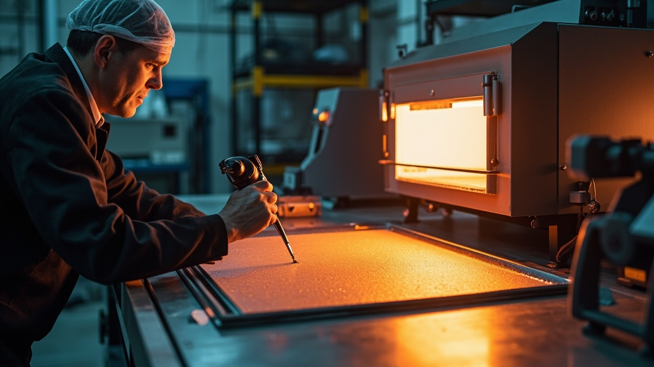
The "performance" of a nano coating is not fixed at the moment of application, but is truly locked in during the film formation and curing stage. For the same formulation, different curing temperature, time, and heating curve can result in vastly different final hardness, adhesion, hydrophobic angle, and durability; while the nano-scale film thickness (nm to µm) directly determines the protection threshold and signal/heat dissipation behavior. Therefore, understanding "how the liquid phase becomes a stable solid phase, how energy is input, and how thickness is controlled" is the only way from laboratory to mass production line.
Focusing on functional coating R&D and industrialization, Kexin New Materials (kexinMaterials) has accumulated a large amount of process window data on the matching of nano ceramics, aerogel composites, and various curing processes. This article combines public TDS and nano composite coating curing research to systematically break down the film formation path, curing method comparison, film thickness control, and inspection methods of nano coatings, for engineers' reference when implementing formulations.
I. Film Formation Methods: Three Paths from Liquid to Solid Phase
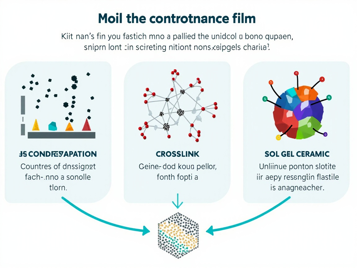
The "film formation" of a nano coating essentially means the liquid precursor transforms into a continuous, dense, well-adhered solid thin film. By mechanism, it can be divided into three types:
- Physical drying type: After solvent or water evaporation, resin/particles pile up to form a film. The process is simplest (e.g., single-component aerogel ceramic coating air-cured at room temperature), but crosslink density and solvent resistance are usually weaker than chemically crosslinked systems;
- Chemical crosslinking type: Two-component (e.g., —NCO and —OH) or single-component moisture-cured, undergoing addition polymerization to form a 3D network, with better hardness and chemical resistance, but subject to pot life and mixing ratio constraints;
- Sol-gel ceramicization type: Precursor (e.g., silane/polysilazane) hydrolyzes and condenses to form an inorganic network, then undergoes heat treatment for "ceramicization". For example, the YC-8703 hydrophobic self-cleaning nano composite ceramic coating in the public TDS is specified as "7-day ceramicization" and can be fast-cured by baking at 150℃ for 30 min, with hardness of 6–7H and long-term service temperature -50℃—400℃.
Engineering note: The curing method must match the film formation mechanism. Baking a coating that "relies on solvent evaporation" at high temperature may cause cracking; leaving a system that "requires chemical crosslinking" at room temperature for a long time may never fully cure.
II. Curing Method Comparison: Room Temperature / IR / Baking / UV
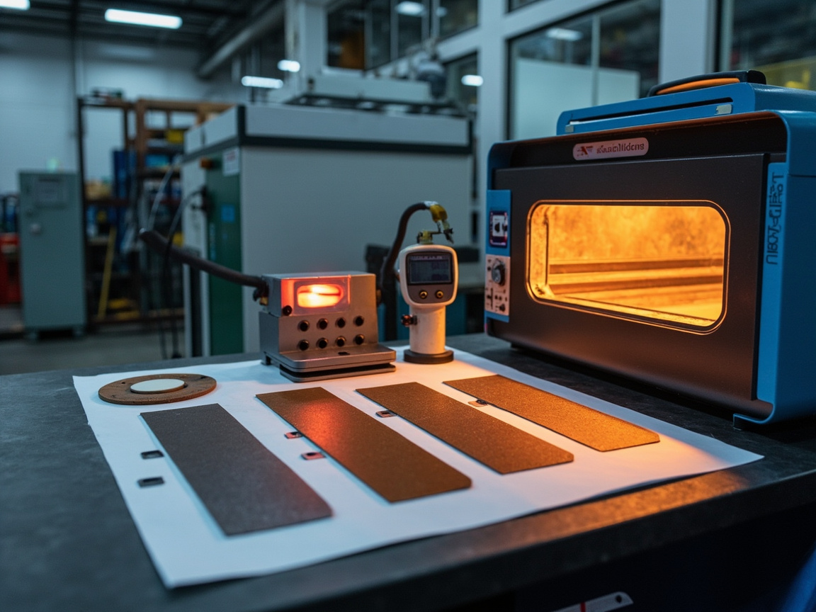
Curing essentially means "input energy to drive crosslinking or ceramicization". Different energy input methods involve trade-offs in cycle, energy consumption, penetration depth, and stress. According to a review of nano composite coating curing process research, a typical comparison is:
| Dimension | Thermal curing (baking/oven) | UV curing (photoinitiation) |
|---|---|---|
| Typical cycle | 30 min – 24 h | 10 s – 5 min |
| Energy consumption | High | Low |
| Substrate limitation | Must be heat-resistant | Must be UV-transmissive or surface-only |
| Penetration/overall curing | Unlimited thickness (bulk curing) | Limited by UV penetration depth |
| Residual stress | Higher (thermal expansion mismatch) | Lower (rapid setting) |
| Oxygen inhibition sensitivity | Low | High (surface may be inhibited) |
| Conversion rate (typical) | >90% | 70%–95% (varies with depth) |
For specific nano coating processes, the public TDS provides a wealth of real windows:
- IR (infrared) heat treatment: Onyx Nano Shield (Si-based nano ceramic shield) is specified as initial curing IR heat treatment 1 h or room temperature 2–3 h, with final curing requiring 14 days;
- Room temperature air curing: ECS 1300AG (aerogel + nano ceramic, electronic protection) is room-temperature air cured, can be accelerated by heating, mainly single-pass;
- Baking/high temperature: Gaamp360 (SiO₂-based automotive ceramic coating) withstands temperature up to 600℃, initial curing 24–48 h, fully 5–7 days; YC-8703 can be fast-cured by baking at 150℃ for 30 min;
- Stepwise post-curing: Typical practice in nano composite epoxy research is post-curing at 80℃ for 2 h + 120℃ for 1 h, with 2℃/min heating/cooling to minimize stress.
Practical experience: Many nano coatings are specified as "room-temperature curable", but final properties (hardness, chemical resistance, adhesion) often rely on a longer final curing period (e.g., 7 days, 14 days) or one heating acceleration. Acceptance should not only look at "surface dry", but at "fully cured".
III. Curing Windows and Film Thickness in Real TDS
Placing the public TDS data of several representative nano coatings on the market side by side, one can intuitively see the correlation of "curing method—film thickness—performance":
| Product/system (per public TDS) | Film thickness | Curing method and time | Key performance |
|---|---|---|---|
| Onyx Nano Shield (Si-based nano ceramic shield) | 200–400 nm | Initial IR 1 h or room temp 2–3 h; final 14 days | Pencil hardness 9H; water contact angle 120°; durability ~1 year |
| Gaamp360 (SiO₂-based automotive ceramic) | 1–3 µm | Initial 24–48 h; fully 5–7 days; temp resistant to 600℃ | Hardness 9H; hydrophobic angle 100–120°; durability 2–5 years |
| ECS 1300AG (aerogel + nano ceramic, electronic) | 12–25 µm | Room-temperature air curing, can be accelerated by heating, mainly single-pass | Superhydrophobic, electrically insulating, extremely anti-corrosive; RoHS/REACH/WEEE |
| Re-yingcai automotive paint nano ceramic (YCC05006G) | 80–150 nm | Room/ambient temperature curing | Pencil hardness 8H–9H; neutral salt spray ≥1200 h; temp resistant -45℃~180℃ |
| YC-8703 nano composite ceramic coating | 50–100 µm | Surface dry 2 h, hard dry 24 h, 7 d ceramicization; can be fast-cured at 150℃ for 30 min | Hardness 6–7H; hydrophobic angle ~110°; bonding to substrate >4 MPa; electrical insulation >200 MΩ |
The insight from this table is: Film thickness and curing time are not the more "aggressive" the better. nm-scale thin films (e.g., 80–400 nm) are suitable for mirror hard films on automotive paint/glass, but protection depth is limited; µm-scale (e.g., 12–25 µm, 1–3 µm) is easier to meet standards for electronic insulation and heavy anti-corrosion. When selecting, first determine "how thick is needed to achieve the protection threshold", then reverse-derive the curing process.
IV. Control Logic and Inspection of Film Thickness from nm to µm
The most fascinating yet tricky aspect of nano coatings is that film thickness spans three orders of magnitude from nano to micro. Different deposition processes naturally correspond to different thickness ranges (per review of nano composite coating deposition research):
| Deposition process | Typical thickness range | Uniformity | Applicable geometry |
|---|---|---|---|
| Spray | 5–100 µm | Medium (edge buildup) | Complex 3D |
| Dip | 1–50 µm | Gradient (thinner at top) | Good |
| Spin | 0.1–10 µm | High (center area) | Planar only |
But "how thick the process can coat" is not the same as "how thick the product should be". The engineering constraints that determine film thickness are:
- Lower limit of protection threshold: Below a certain thickness, hydrophobicity/insulation/anti-corrosion no longer meet standards (e.g., PCB conformal coating <25 µm shows significant drop in protection, see the electronics protection topic);
- Upper limit of heat dissipation and flexibility: Too thick affects component heat dissipation, or cracks under large ΔT;
- Uniformity: Spray edge buildup, dip coating thinner at top, spin coating limited to flat surfaces—all these require control by actual measurement rather than visual inspection.
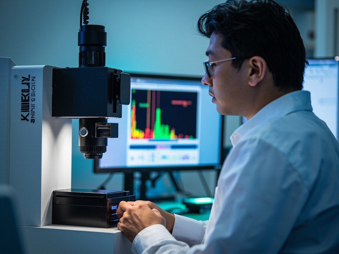
Thickness measurement must match the scale:
- 1–1000 nm: Ellipsometer (Spectroscopic Ellipsometry), non-contact, high precision, suitable for nano ceramic films and wafer-level coatings;
- Tens of nm–hundreds of µm: Stylus Profilometry, quantified via film edge step;
- nm–µm interface: SEM cross-section observation, simultaneously viewing morphology and interface bonding;
- 25–250 µm (conformal coating type): Eddy current thickness measurement or cross-section method, IPC-CC-830 recommends 5–10 points per board.
Key reminder: Nano coating being "thin" is relative to macroscopic coatings. What truly affects performance is the effective dense layer thickness. If local thinning/pinholes occur due to agglomeration or process issues, the entire board protection will "short-circuit" at that point. Therefore, multi-point actual measurement + defect inspection (bubbles, pinholes, bridging) are both indispensable.
V. Cure Degree Determination: Don't Just Look at "Dry or Not"
"Surface dry" "touchable" does not equal "fully cured". Industry commonly uses the following methods to determine the degree of cure:
- FTIR / ATR-FTIR: Track characteristic functional group peak intensity changes, such as consumption of isocyanate —NCO, epoxy groups, silanol groups, and estimate conversion rate by peak area ratio. Research reviews indicate thermal cure conversion usually >90%, UV cure affected by penetration depth about 70%–95%;
- Residual stress (wafer curvature method): Thermal cure often produces higher residual stress due to thermal expansion mismatch, which needs to be mitigated by heating/cooling rates (e.g., 2℃/min);
- Macroscopic performance inference: Pencil hardness (GB/T 6739), adhesion (GB/T 9286), solvent wipe resistance, reaching stable values is considered fully cured;
- DSC/TGA: Detect residual reaction enthalpy and thermal stability.
For nano ceramic coatings, also pay attention to "ceramization degree"—whether the sol-gel network is sufficiently polycondensed, and whether it will absorb moisture due to residual hydroxyl groups. Such hidden indicators often determine long-term durability more than "how many days to dry".
VI. Process Window and Common Defect Control
Defects in the curing and film-forming stages mostly stem from loss of process window control:
| Defect | Typical Cause | Countermeasure |
|---|---|---|
| Orange peel | Spray viscosity too high / distance too far | Recheck TDS viscosity, control 15–25 cm spray distance |
| Bubbles/pinholes | Flux residue outgassing, coating too thick, insufficient interlayer flash-off | Strengthen cleaning, control thickness, extend flash-off |
| Thermal cycle cracking | Rigid coating + large ΔT / flexible substrate | Change to flexible formulation, reduce film thickness, moderate heating/cooling |
| Under-cure | Room temperature storage not reaching final cure period | Set final cure period or heat acceleration, verify with FTIR |
| Agglomeration/non-uniform | Poor nanoparticle dispersion | Surface modification + ultrasonic dispersion, see characterization topic |
In mass production process design, Kexin New Materials (kexinMaterials) usually advises customers to write "surface treatment—coating parameters—cure curve—thickness measurement points—acceptance criteria" into a process card, rather than relying on experience to "just coat and see". For example, for electronic/automotive parts requiring fast delivery, 150℃ short-time baking can be used to accelerate ceramization (e.g., YC-8703's 30 min fast cure), but film thickness and cure degree must be confirmed simultaneously with ellipsometry/stylus profilometry to avoid "surface dry inside raw". For quantitative determination of film thickness and morphology, further refer to our topic on Detection and Characterization of Nano Coating: Particle Size, Zeta, Film Thickness and Hardness.
VII. Summary of Selection and Process Recommendations
Turn the full text into an executable checklist:
- First set film thickness target: Protection (anti-corrosion/insulation) looks at lower limit, heat dissipation/flexibility looks at upper limit, reverse-derive process by mechanism;
- Then select cure method: Room temperature if possible (low energy, low stress), use IR/baking to speed up but final cure period cannot be omitted;
- Match substrate heat resistance: Use caution with high-temperature baking for flexible/heat-sensitive substrates, prioritize room temperature or low-power IR;
- Accept by data: Ellipsometry/stylus profilometry for thickness + FTIR for cure degree + hardness/adhesion + hydrophobic angle, all indispensable;
- Control defects: Cleaning, viscosity, flash-off, heating/cooling rate, write into process card.
When the project also involves determination of "whether hydrophobic self-cleaning meets standard", it is recommended to read further Nano Coating Hydrophobic Angle and Rolling Angle; when entering the on-site construction implementation stage, combine with Nano Coating Construction Process: Surface Treatment, Coating and Curing Window for unified planning.
Final reminder: Don't treat "fast cure" as the only goal. Fast cure often comes at the cost of higher energy consumption, greater thermal stress or limited penetration; truly robust mass production is finding a balance among "performance met, acceptable takt, controllable stress, worry-free compliance". Stringing the film-forming mechanism, cure comparison, film thickness control and dispersion gating of this article into a process chain is more efficient than repeated trial and error, and can more stably deliver the "thin yet strong" of nano coatings to the client.
VIII. Cure Kinetics: Heating Curve, Reaction Rate and Residual Stress
Curing is not "just heat and done", but a kinetic curve of "temperature—time—conversion rate". Grasping this curve avoids hidden defects:
- Trap of too fast heating: Surface reaches reaction temperature first and rapidly skins, "sealing" internal solvent or unreacted monomer under the film, which escapes later forming bubbles, pinholes, or even intra-layer voids; meanwhile the surface dry skin hinders subsequent component diffusion, causing "external cured, inner raw".
- Meaning of stepwise heating: Typical practice in nano composite epoxy research is 80℃ 2 h + 120℃ 1 h post-cure, with 2℃/min heating/cooling, aimed at letting reaction proceed uniformly, letting volatiles escape leisurely, and keeping thermal stress within tolerable range.
- Source of residual stress: One is coefficient of thermal expansion (CTE) mismatch between coating and substrate, the other is curing volume shrinkage. Thermal cure experiences higher temperature and larger temperature difference, so residual stress is usually higher than UV cure (research reviews indicate thermal cure conversion often >90% but stress higher, UV conversion 70%–95% but stress lower). Excessive residual stress manifests as reduced adhesion, edge lifting or thermal cycle cracking.
- How to quantify residual stress: Commonly wafer curvature method (wafer curvature / Stony formula), reverse-calculating in-film stress via substrate curvature before and after curing; also nano indentation and scratch critical load can indirectly assess interface bonding margin. For flexible substrates, a stress release layer (e.g., flexible primer) can be introduced between coating and substrate to buffer.
- Process countermeasure strategy: Decouple "high stress" and "fast takt"—first use low temperature long time to initially form network, then short high temperature to complete final crosslinking; or within allowable range reduce film thickness, select lower shrinkage monomer/precursor. Essentially, residual stress management is the hidden main line of cure curve design, more worthy of attention than "how long to bake".
- Room temperature vs high temperature trade-off: Room temperature cure has lowest stress, most energy-saving, but longest cycle; high temperature/IR accelerates but stress and substrate heat resistance limited. Practical compromise is often "low temperature long time" or "IR local heating to reduce overall heating".
IX. Essential Differences Between Nano Coating and Traditional Paint Curing
Many engineers apply traditional industrial paint experience to nano coatings, easily stepping into pitfalls. Key differences in cure logic:
| Dimension | Traditional Industrial/Automotive Coating | Nano Coating |
|---|---|---|
| Typical film thickness | µm level (tens to hundreds of µm) | nm–µm level (80 nm to tens of µm) |
| Film formation dominant | Solvent evaporation + oxidation/crosslinking | Sol-gel ceramic conversion / chemical crosslinking / nano stacking |
| Drying determination | Surface dry / hard dry (e.g., GB/T 1728 surface dry ≤ 4 h, hard dry ≤ 24 h are common) | "Surface dry" is far from fully cured, often requiring 7–14 days for final stage |
| Detection scale | Coating thickness gauge, cross-cut, hardness | Additionally requires ellipsometry/profilometer/SEM to see nm scale |
| Uniformity risk | Sagging, orange peel | Nano agglomeration, pinholes more easily cause "local short circuit" |
In short, traditional paint concerns "whether it's dry, whether it flows unevenly", while nano coating also needs to check "whether ceramic conversion is sufficient, whether nano dispersion is uniform". Directly applying the latter's acceptance criteria to the former's experience often misses the most fatal hidden defects.
Precisely because of the scale difference, the "surface dry / hard dry" determination of traditional paint (e.g., GB/T 1728) cannot be directly transferred to nano coatings: the "hard dry" of nano ceramics often corresponds to whether the sol-gel network is sufficiently polycondensed and whether chemical crosslinking has reached stable conversion, rather than simply "solvent evaporated and not sticky". This is also why the previous text emphasized FTIR curing degree and final curing period—using the macro paint's "dry" to cover the nano coating's "form" is a typical experience mismatch.
X. Examples of Typical Process Curves (Real TDS Perspective)
Summarize the public TDS curing windows of representative nano coatings on the market again, emphasizing "final curing period cannot be omitted":
- Onyx Nano Shield (Si-based): Initial curing IR 1 h or room temperature 2–3 h, but final curing requires 14 days—this means the "feel hardness" upon leaving factory and the "full performance" after 14 days are not the same;
- Gaamp360 (SiO₂-based): Initial 24–48 h, full 5–7 days, temperature resistance up to 600℃, durability 2–5 years;
- ECS 1300AG (aerogel + ceramic, electronic): Room temperature air curing, can be accelerated by heating, mainly single coat, suitable for temperature-sensitive PCB;
- YC-8703 (nano composite ceramic coating): Surface dry 2 h, hard dry 24 h, 7 d ceramic conversion, can be fast cured by baking at 150℃ for 30 min, hardness 6–7H;
- Re-yingcai automotive paint nano ceramic: 80–150 nm thin film, room/ambient temperature curing achieves 8H–9H and ≥1200 h salt spray.
The common rule is: Room temperature operable ≠ room temperature final performance. If the production tempo does not allow 7–14 days of natural curing, controlled heating (IR/oven) must be used for "accelerated but final-cure-equivalent" treatment, and the equivalence verified by FTIR/hardness, rather than simply "baked dry is fine".
XI. Production Process Card and Implementation Coordination
To turn film forming and curing from "experience" into "replicable process", the most effective is a process card, suggested to include at least:
- Surface treatment grade: Sandblasting Sa2.5 (e.g., 46-mesh white corundum) or grinding/cleaning threshold, clarifying surface energy requirements;
- Coating parameters: Spray pressure/distance/speed, or dip-coating withdrawal speed, or spin-coating rpm—determining film thickness range;
- Curing curve: Temperature—time nodes (e.g., 80℃×2 h → 120℃×1 h, 2℃/min ramp), and water/dust avoidance window;
- Thickness measurement points: Select ellipsometry/profilometer/eddy current by scale, mark sampling positions and frequency;
- Acceptance thresholds: Pencil hardness (GB/T 6739), cross-cut adhesion (GB/T 9286), contact angle, FTIR curing degree, salt spray/humidity resistance;
- Abnormal handling: Traceability path for orange peel/bubbles/cracking (see defect table in Section VI).
- Traceability and sample retention: Record original temperature—time data of curing curve, measured film thickness and first-piece samples for each batch, establish traceable archive, facilitate quick locating of material, process or substrate issue when client-side failure occurs. The essence of stable mass production is to turn "do it right once" into "can do it right every time", and the traceability system is the bottom-line guarantee for this goal.
When importing the process card into the production line, Kexin New Materials (kexinMaterials) can provide full support from formulation, curing curve calibration to third-party testing connection, helping customers move the stable mass production of "nano thin coating" from lab to workshop, rather than stopping at samples. For quantitative determination of film thickness and morphology, further refer to Detection and Characterization of Nano Coating: Particle Size, Zeta, Film Thickness and Hardness; for on-site construction stage, combine with Nano Coating Construction Process: Surface Treatment, Coating and Curing Window for unified planning.
XII. Curing Equipment Selection: Trade-offs among IR Lamps, Convection Ovens and UV Furnaces
When implementing the curing process into the workshop, the first choice is "what equipment to use for heating". The trade-off logic of three mainstream equipment is as follows:
| Equipment | Heating / Tempo | Uniformity | Applicable System | Main Limitation |
|---|---|---|---|---|
| IR infrared lamp | Fast (local second-level heating) | Depends on lamp array and distance, prone to uneven | Thin layer, line, local acceleration (e.g., Onyx IR 1 h) | Temperature field hard to be absolutely uniform, need multi-point temperature measurement |
| Convection oven | Slow but controllable curve | Overall good, can step-control temperature | Batch, thick film, need precise curve (e.g., 80→120℃ post-curing) | High energy consumption, slow heating, thermal stress needs attention |
| UV curing furnace | Extremely fast (10 s–5 min) | Surface good | UV-initiated acrylate nano system | Limited penetration depth, oxygen inhibition, not suitable for ceramic conversion thermal reaction |
The selection matrix can be simplified as: Need fast and thin → IR; Need batch and precise curve → convection oven; Need extreme tempo and UV-curable system → UV furnace. For sol-gel ceramic conversion types (requiring thermal polycondensation), UV is usually not applicable, still mainly IR/oven. Regardless of equipment, it is recommended to deploy points to measure temperature field and record "temperature—time" curve, as part of the process card, to avoid deviation between "set 120℃" and "actual surface 120℃". Equipment also needs periodic calibration (e.g., IR lamp attenuation, oven uniformity, UV radiometer drift), incorporating hardware aging into maintenance plan to maintain long-term consistency.
XIII. Dispersion Stability: The Most Easily Overlooked Variable Before Curing
Many nano coating failures do not occur at the "curing" step, but earlier—the dispersion state of nanoparticles before film forming determines the uniformity of the final film. Nano particles have huge specific surface area and extremely high surface energy, naturally tending to agglomerate to reduce surface energy; once agglomerated, three types of chain problems appear:
- Non-uniform film: Large agglomerates form local "islands" or rough points in the film, destroying nm-level flatness and causing stress concentration;
- Pinholes and short circuit: Micro-pores left after agglomerate detachment make the protective layer lose local continuous density, electronic coating leaks here, anti-corrosion coating starts corroding from here;
- Performance not up to standard: The hydrophobic/reinforcement/low-k effects that should be provided by uniform nano structure are diluted by agglomeration, measured contact angle, hardness, resistivity all decline.
Conventional engineering means to inhibit agglomeration include: surface modification of particles (silylation, coupling agent) to reduce surface energy; adding dispersant and combining with ultrasonic/shear dispersion; controlling solvent polarity and solid content to avoid secondary flocculation; and monitoring dispersion stability with Zeta potential and DLS particle size distribution before coating (see characterization topic). An experienced practice is to "treat dispersion as half of the formulation"—no matter how good the film forming and curing process is, it cannot save an already agglomerated slurry. This is why the mass production process card should include "particle size/Zeta sampling of dispersion batch", not just watch the curing curve.
At the mass production site, it is recommended to treat dispersion quality as a gate item rather than post-inspection: each batch of slurry measured once for DLS particle size distribution and Zeta potential before coating, set "D50/D90 upper limit" and "Zeta absolute value lower limit", if exceeded, reflux re-dispersion or downgrade use; control shear and standing time during packaging and temporary storage to avoid secondary flocculation from long-distance transport or long storage. For water-based and solvent-based nano systems, the former is more prone to flocculation due to ionic strength change, the latter needs more to prevent concentration drift from solvent evaporation—gate rules should be set separately by system. Turning "invisible dispersion" into "quantifiable release standard" is the key leap for nano coating from sample to stable mass production. Ignoring it, no matter how precise the curing curve is, it only "fixes the shape" of an already non-uniform film.
FAQ
1. Is the nano coating "surface dry" means it is fully cured?
Not necessarily. Surface dry only indicates solvent evaporation or surface skinning; chemical crosslinking or sol-gel ceramic conversion often requires a longer final curing period (e.g., 7 days, 14 days) or one heating acceleration. Acceptance should be comprehensively determined by hardness, adhesion, solvent resistance, and FTIR curing degree, rather than by touch-dry non-stickiness.
2. How to choose among the four curing methods: room temperature, IR, baking, and UV?
Room temperature saves the most energy and has low stress, suitable for heat-sensitive/flexible substrates; IR and baking can accelerate and improve crosslinking density, but are limited by substrate heat resistance; UV is extremely fast and low-energy, yet affected by penetration depth and oxygen inhibition, more suitable for thin layers or surface layers. The choice depends on substrate, film thickness, and takt requirements.
3. What is the typical film thickness of nano coatings?
The range is very wide: automotive paint/glass ceramic hard film can be 80–400 nm, electronic aerogel ceramic about 12–25 µm, SiO₂ automotive ceramic 1–3 µm, nano composite ceramic coating 50–100 µm. The core is "achieving the protection threshold without affecting heat dissipation and flexibility", not the thicker the better.
4. How to measure nm-level film thickness?
For 1–1000 nm, spectroscopic ellipsometry is preferred, non-contact and high precision; for tens of nm to hundreds of µm, step profiler/surface profilometer; for nm–µm interface and morphology, SEM cross-section; for conformal coating types (25–250 µm), eddy current thickness measurement or cross-section method.
5. What method is used to determine curing degree?
Most commonly ATR-FTIR tracks the consumption of characteristic functional groups to estimate conversion rate (thermal curing often >90%, UV affected by depth 70%–95%); supplemented by residual stress (wafer curvature), pencil hardness, adhesion, and DSC/TGA. For sol-gel ceramic coatings, it is also necessary to check whether network condensation is sufficient and whether residual hydroxyl groups are hygroscopic.
6. Why does my nano coating have orange peel, bubbling, or cracking?
Orange peel is mostly due to uncontrolled spraying viscosity and distance; bubbles/pinholes often come from substrate residual outgassing or excessive coating thickness and insufficient flash-off; thermal cycle cracking is mostly due to rigid coating encountering large ΔT or flexible substrate. The countermeasures are to strengthen cleaning, control thickness, extend flash-off, moderate heating and cooling, and write the parameters into the process card.
7. Does nanoparticle agglomeration affect film formation?
Yes. Nanoparticles have high surface energy and easily agglomerate, leading to uneven film, local pinholes or excessive thickness, destroying protection continuity. It needs to be solved by surface modification, dispersant, and ultrasonic dispersion, which is also why "half of the nano coating formulation is in dispersion".
8. Can high-temperature baking accelerate all nano coatings?
No. It must be based on the film-forming mechanism of the formulation and substrate heat resistance: solvent evaporation type and some ceramic systems can be heated to accelerate (e.g., 150℃ 30 min fast cure), but chemically crosslinked two-component has pot life and mixing ratio constraints, and heat-sensitive/flexible substrates may also be burned. Everything is subject to TDS and process validation.
9. The faster the heating, the higher the curing efficiency, the better?
No. Too fast heating will cause the surface to skin first, internal bubbles and "external cured but inner raw core", and increase thermal mismatch residual stress, which instead reduces adhesion and long-term reliability. Stepwise heating is recommended (e.g., 80℃×2 h then 120℃×1 h, 2℃/min ramp), and confirm conversion rate with FTIR.
10. Do nano coatings also need to measure VOC like traditional paint?
It depends on the system and application. Industrial protective coating is constrained by VOC limits such as GB 30981-2020; single-component aerogel ceramic or water-based nano systems often have low solvent content, but still need to be confirmed according to product TDS and actual regulations (such as emission requirements of coating process), and cannot be defaulted exempt because of "nano". When selecting, VOC and hazardous substance data should be requested from the supplier.
Further Reading
- Nano Coating Hydrophobic Angle and Rolling Angle: Characterization and Self-cleaning Significance: Understand the test method of hydrophobic angle after curing, to judge "true superhydrophobic" or "false value".
- Nano Coating Construction Process: Surface Treatment, Coating and Curing Window: Implement film-forming curing parameters into the unified planning of on-site construction and curing window.
- Detection and Characterization of Nano Coating: Particle Size, Zeta, Film Thickness and Hardness: Supplement technical details of quantitative detection means such as ellipsometry, step profiler, Zeta, and hardness.