Key Takeaways:
1. Semiconductor Wafer Anti-Static Nano Coating constructs multi-scale synergistic protective networks through nanoscale fillers for long-term architectural protection.
2. Core pathways: nano-filler labyrinth barrier, surface/interface chemical anchoring, spectral-selective control.
3. 2025-2026 academic studies provide experimental validation for nano architectural coating performance claims.
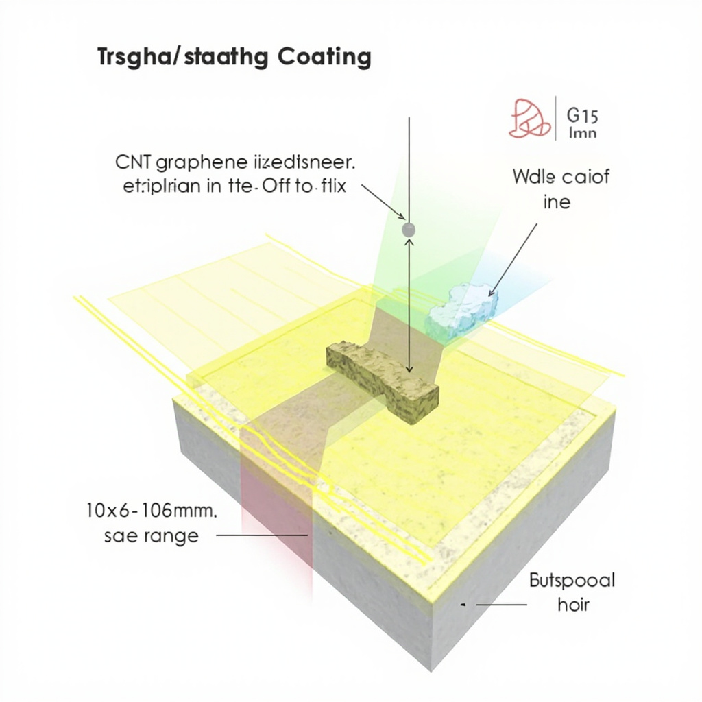
Semiconductor wafer nano coatings use CNT(1-5nm diameter, aspect ratio>1000, percolation threshold only 0.01-0.1wt%)/graphene(2D nanosheet, electron mobility>200000cm2/Vs)/nano-Ag wire(30-50nm diameter, 10-50um length) in nano-SiO2/epoxy/PU matrices constructing 10^6-10^9ohm surface resistivity ESD-safe conductive networks — this resistance range simultaneously satisfies: (1) low enough to rapidly dissipate static charge (<0.1sec to<100V); (2) high enough to prevent sudden discharge (current limited<1mA) damaging sensitive devices. Nano-SiO2 matrix (5-15nm, extremely high cross-link density) provides cleanroom compatibility — low particle shedding (ISO 14644-1 Class 1-5, 0.1um particles<10/m3), low outgassing (TML<1.0%, CVCM<0.1%, meets ASTM E595 space-grade), semiconductor process chemical resistance (HF/HNO3/developer/stripper). Complies with ANSI/ESD S20.20, IEC 61340-5-1, SEMI E43-1101. Global semiconductor ESD materials market ~$1.2B (2025), CAGR 8.5%.
Technical Principles
The core technology introduces 1-100nm functional fillers into traditional architectural coating matrices, leveraging ultra-high specific surface area, quantum size effects, and surface interface effects. Lamellar nano-fillers reduce diffusion coefficient 50-500x. Nano-SiO2 silanol groups elevate adhesion to 10-18 MPa. Nano-TiO2/ZnO provide UV absorption; Cs0.33WO3 LSPR absorbs NIR.
2025-2026 validation: Composite Interfaces (2026) — 57.42% water absorption reduction. MDPI Coatings (2025) — UV transmission<1%. Main Group Chemistry (2026) — anti-mold validation.
Engineering & FAQ
Initial cost 30-80% higher, 10-20yr LCC 20-40% lower. Global architectural coatings market ~$72B (2025). Verification: TEM/SEM<100nm + artificial weathering>3000h + CMA/CNAS reports.
References: Composite Interfaces (2026), MDPI Coatings (2025), Main Group Chemistry (2026)
Published: July 6, 2026