
The reliable lifespan of electronic devices increasingly depends on an invisible "thin layer" — electronic triple-proof nano coating. Unlike conformal coatings that are often tens of microns thick, nano coatings typically have a film thickness between 100 nm and 1 micron, yet with their molecular-scale dense structure and extremely low surface energy, they block liquids and contaminants such as moisture, salt spray, sulfides, sweat, and coffee stains from reaching the circuit board. From smartphone motherboards, wearable devices, automotive ECUs, to industrial sensors and LED modules, ultra-thin nano protection is becoming one of the mainstream approaches for high-end electronic protection.
As a technical supplier in the field of electronic protection materials, Kexin New Materials (kexinMaterials) has long tracked application data of nano coatings on PCBs and precision components. This article thoroughly explains "electronic triple-proof nano coating" from failure mechanisms, technical routes, hydrophobic mechanisms, standard characterization to construction selection, helping engineers make rational choices among thinning, high reliability, and repairability.
I. What is Electronic Triple-proof Nano Coating: The Essential Difference from Conformal Coating
Traditional conformal coating, according to IPC-CC-830 / IEC 61086, typically has a film thickness of 25–200 µm, isolating the circuit from the outside by "physical coverage". Its advantages are scratch resistance, chemical resistance, and selective thick coating; its disadvantages are that the film thickness affects heat dissipation and component conformality, repair requires stripping, and it imposes stress on some miniature components.
Nano coating follows a different logic: it builds a dense, low-surface-energy, high-insulation thin film on the substrate surface using nano-scale (10⁻⁹ m) functional molecules, with a typical film thickness of 100 nm–1 µm, about 1/50 to 1/200 of conformal coating. Its protection does not rely on "thickness accumulation", but on:
- Dense pinhole-free structure: Sol-gel or vapor-deposited films are continuous and defect-free, preventing liquid capillary penetration;
- Extremely low surface energy: Fluorosilicone groups give a water contact angle of 100°–120°, and droplets roll off taking pollutants away;
- High insulation: The film's volume resistivity can reach the order of 10¹⁴–10¹⁶ Ω·cm (according to the principle of GB/T 1410 volume resistivity test), blocking leakage current;
- Good conformality: Vapor-phase processes can uniformly coat 3D structures without increasing dimensions.
The relationship between the two can be understood as "thick cotton-padded jacket" and "nano raincoat": the former is heavy and durable, the latter is light and close-fitting. In actual engineering, the two are often complementary — critical solder joints or exposed metal use conformal coating, while the whole device or module level uses nano coating as secondary protection.

II. Electronic Failure Mechanisms: What Nano Coating Protects Against
To understand the value of nano coatings, first look at how exposed or under-protected electronics fail in real environments:
- Electrochemical Migration (ECM): Under moisture + bias voltage (e.g., several volts between adjacent traces), copper and silver ions migrate along the surface water film and reduce to dendrites, eventually bridging and short-circuiting. This is the main cause of consumer electronics "breaking upon water ingress".
- Condensation and bridging: Day-night temperature differences or equipment start-stop cause condensation on the board surface forming a continuous water film, dropping insulation resistance from GΩ to MΩ or even lower, causing malfunction.
- Salt spray corrosion: In coastal and automotive environments, Cl⁻ penetrates and corrodes solder joints, copper foil, and silver wires, generating green rust (basic copper carbonate) or blackened silver.
- Sulfidation/corrosive gases: H₂S, SO₂, NOₓ react with silver and tin to form insulating or poorly conductive sulfides (e.g., Ag₂S), causing contact resistance to surge and signal loss.
- Sweat and liquid splashing: Human sweat contains NaCl and lactic acid; coffee and beverages contain sugars and ions, which penetrate connectors causing chronic corrosion.
- Mold and dust: Under high temperature and humidity, organic residues breed mold damaging insulation, and conductive dust bridges pins.
Nano coatings, through the triple mechanism of "hydrophobic + dense + high insulation", fundamentally weaken the above paths: water does not wet the board surface (Cassie-Baxter state), and even with trace moisture there is a lack of continuous ion channels, so ECM and salt spray corrosion are greatly suppressed.
III. Mainstream Nano Coating Technical Routes
3.1 Sol-Gel Method
Using silane, titanate, or aluminate precursors to hydrolyze and condense, forming SiO₂ / TiO₂-like inorganic-organic hybrid networks on the substrate surface. Advantages are strong adhesion, high hardness, and possible fluorination modification to enhance hydrophobicity; disadvantage is the need for bake curing (80–150℃), limiting temperature-sensitive components. Film thickness can be controlled at 200 nm–2 µm. Commonly used for LED brackets, connectors, sensor housings.
3.2 Fluorosilicone Self-Assembled Monolayer (SAM)
Fluorosilane (e.g., perfluoroalkyl siloxane) self-assembles into a monolayer on hydroxylated surfaces via Si–O–M bonds, only 1–5 nm thick but with extremely low surface energy. It can give a water contact angle above 110° and rolling angle <10°, exhibiting the "lotus leaf effect". SAM barely adds weight or blocks holes, suitable for MEMS, miniature microphones, precision optoelectronic devices. Its weakness is poor mechanical wear resistance, requiring配合 with a base layer protection.
3.3 Vapor Deposition: Parylene and Fluoropolymer
Poly(p-xylylene) (Parylene, XY) is pyrolyzed from dimer and vapor-deposited at room temperature, with no dead corners, uniform, and excellent chemical resistance, being a benchmark for high-end electronic protection, but with large equipment investment and difficult repair. There is also solvent-free fluorinated acrylate plasma polymerization, which can generate nano fluorinated films on plastics and metals, with clean process and near-zero VOC.
3.4 Atomic Layer Deposition (ALD)
ALD grows layer by layer via self-limiting surface reactions, with film thickness precise to single atomic layers (Å level), dense and pinhole-free, commonly used for semiconductor device passivation and water/oxygen barrier layers (e.g., OLED encapsulation). In the PCB field, it is frontier, high cost, mostly used in military, aerospace, and medical electronics.
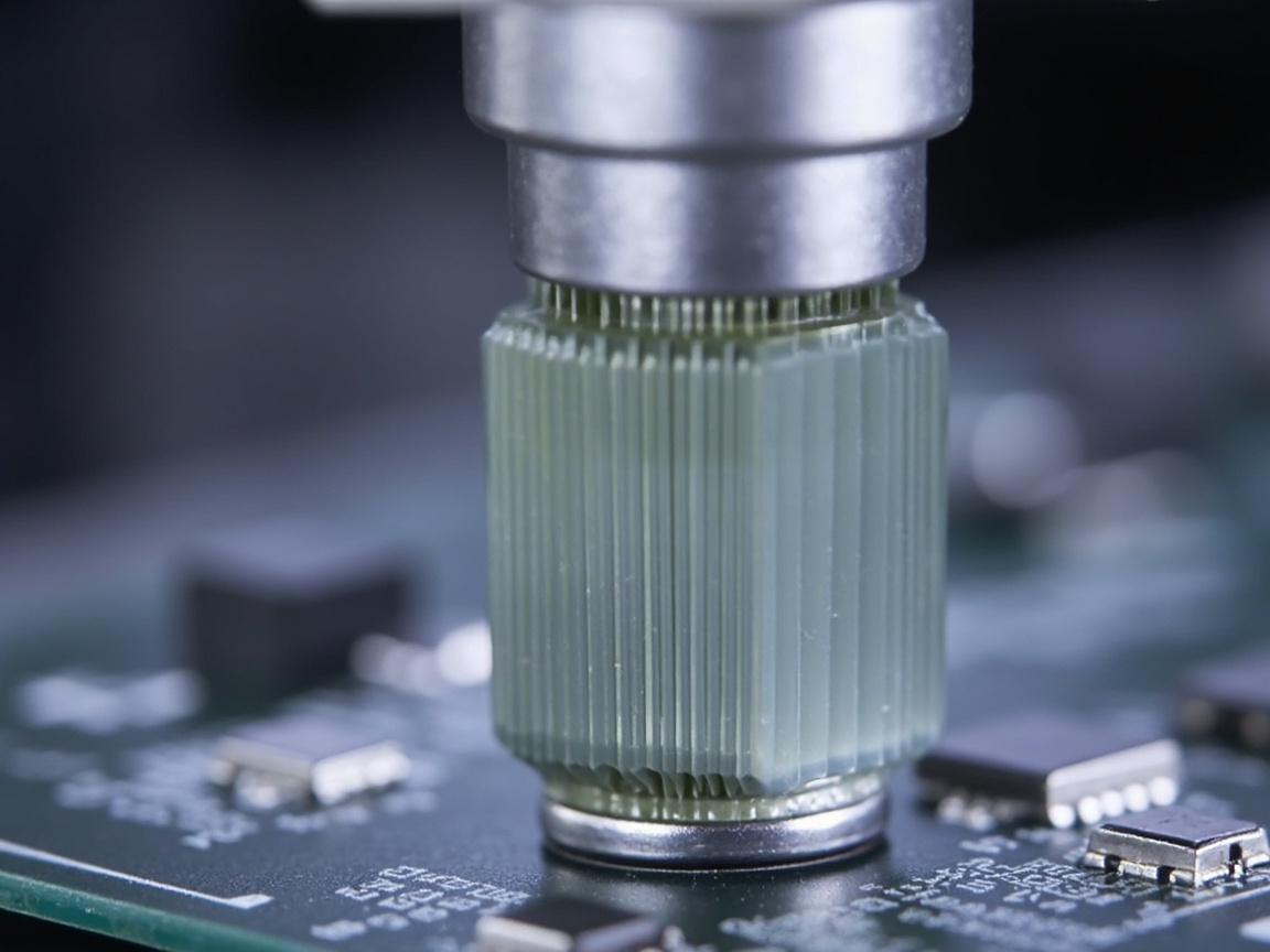
IV. Hydrophobic Mechanism and Contact Angle: Why Test Methods Must Be Noted for the Numbers
The "hydrophobicity" of nano coatings is not metaphysics, but the coupled result of surface chemical energy and micro-nano morphology:
- Wenzel state: Droplet immerses into the pits of a rough surface, contact angle is amplified but droplet remains sticky;
- Cassie-Baxter state: Air is trapped below the droplet, forming an "air cushion", with high contact angle and small rolling angle, the ideal protective state.
Engineering uses water contact angle (CA) and rolling angle (SA) for characterization: according to ASTM D7334 (contact angle measurement) or GB/T 30693-2014 (water contact angle of plastic films) principles, high-quality electronic nano coatings have water contact angle 100°–120°, rolling angle <15°, meaning droplets easily roll off without residue. It must be emphasized: contact angle depends on substrate roughness and test liquid (pure water/salt water/simulated sweat); claiming "hydrophobic 120°" must note the system and test method to avoid exaggeration.
V. Performance Characterization and Referenced Standards
Electronic triple-proof nano coatings need verification in multiple dimensions, key standards include:
- Insulation and resistance: Dielectric strength according to GB/T 1408.1 "Test method for electric strength of insulating materials"; volume/surface resistivity according to GB/T 1410 "Test method for volume resistance and surface resistance of solid insulating materials"; the goal is that the film does not reduce the original circuit insulation margin.
- Triple-proof qualification: Nano coatings often serve as a supplement to the triple-proof system, and can still refer to IPC-CC-830 / IEC 61086 "Electrical insulating compounds for printed boards" for humidity-heat post insulation resistance, salt spray resistance, etc. qualification.
- Salt spray: Neutral salt spray (NSS) according to GB/T 10125 / ISO 9227, PCB after coating often requires 96–500 h without bridging or corrosion.
- Constant damp heat: According to GB/T 2423.3 (IEC 60068-2-78) or GB/T 2423.4 alternating damp heat, assessing insulation resistance retention under high temperature and humidity.
- Temperature cycling: According to GB/T 2423.22 (IEC 60068-2-14), verifying the thermal expansion matching of film and substrate, no cracking or detachment.
- Liquid resistance: Sweat, coffee, salt water immersion, evaluating appearance and resistance changes.
These standards constitute the evidence chain that "electronic triple-proof nano coating" can be referenced by customers and certification bodies, and are also the core that must be cited in technical articles.
VI. Comparison between Nano Coating and Traditional Conformal Coating
The following table compares the two protection schemes from an engineering dimension for easy selection:
| Comparison Dimension | Traditional Conformal Coating (AR/UR/SR/XY) | Electronic Triple-proof Nano Coating | Engineering Meaning |
|---|---|---|---|
| Typical Film Thickness | 25–200 µm | 100 nm–1 µm | Nano layer adds no weight, blocks no holes |
| Protection Mechanism | Physical coverage isolation | Dense + low surface energy + high insulation | Nano layer relies on chemistry and structure rather than thickness |
| Surface State | Visible film, slightly thickened | Nearly invisible | Suitable for thinning, transparent parts |
| Hydrophobic performance | General (depends on formulation) | Contact angle 100°–120° | Better splash resistance and anti-condensation |
| Impact on heat dissipation | Has thermal resistance | Minimal | Friendlier to high-power devices |
| Repairability | Removable by solvent/mechanical stripping | SAM type difficult, sol-gel can be locally removed | Different maintenance strategies |
| Process equipment | Mature coating machines | High investment in vapor-phase/plasma equipment | Large difference in scale cost |
| Applicable scenarios | Whole board, solder joints | Modules, connectors, precision parts | Complementary rather than substitution |
Note: Nano coating does not "replace" conformal coating, but rather serves as graded protection—using nano layer for whole-device waterproofing, and conformal coating for critical solder joints and power devices (see conformal coating for electrical control box).
VII. Typical Application Scenarios
- Consumer electronics: Mobile phone mainboards, TWS earphones, smart watches use nano waterproofing (IPX2–IPX4 splash protection) to reduce water-damage return rate.
- Automotive electronics: Cockpit domain controllers, sensors, camera modules under −40–105℃ and salt spray environment, nano layer combined with conformal coating improves lifespan.
- Industrial and outdoor: PLC, transmitters, meteorological sensors long-term outdoor, nano hydrophobic anti-condensation.
- LED and lighting: LED brackets, power modules prevent sulfidation blackening (silver reflector cup sulfidation is an industry challenge).
- Medical and wearable: Skin-contact devices resist sweat corrosion.
- New energy: BMS acquisition boards, charging module circuit boards (forming secondary protection with outdoor weather-resistant coating for charging piles) improve damp-heat reliability.
VIII. Construction Process and Film Thickness Control
Success of nano coating is seven-tenths in pre-treatment:
- Plasma cleaning: Remove organic contaminants, activate surface hydroxyl groups, improve adhesion, is the prerequisite for vapor-phase and SAM processes.
- Coating methods: Sol-gel can use dip coating, spray coating, brush coating; vapor-phase process uses vacuum chamber deposition; SAM uses solution immersion followed by baking.
- Curing: Sol-gel baked at 80–150℃; plasma polymerization at room temperature; ALD slightly higher temperature but can be as low as 100℃ level.
- Film thickness control: Monitor with ellipsometer, step profiler or XRF; target value needs to balance protection and electrical clearance.
- Masking and selectivity: Connector gold fingers, test points need masking to avoid affecting contact resistance.
IX. VOC and Environmental Compliance
Electronic protection materials are also subject to environmental constraints. According to GB 30981-2020 "Limit of Harmful Substances in Industrial Protective Coatings", VOC limits for industrial protective coatings are tightening; nano coatings, mostly solvent-free or water-based systems, have significantly lower VOC than solvent-based conformal coatings. Kexin New Materials (kexinMaterials)'s R&D on nano hybridization and water-based precursors is precisely to maintain hydrophobic insulation performance while meeting low VOC requirements, echoing the green manufacturing trend in electronics.
X. Selection Recommendations
Engineers can make three-step decisions on "electronic conformal protection" schemes:
- Look at environmental level: For splash protection only, nano layer is sufficient; for long-term salt spray/immersion, choose conformal coating or composite of both.
- Look at component density: High-density miniature parts, transparent parts prioritize nano layer; large solder joints, power devices use conformal coating.
- Look at mass production and cost: Vapor-phase equipment has high CAPEX but low unit cost, suitable for large volume; small batches use sol-gel spray for more flexibility.
Overall, Kexin New Materials (kexinMaterials) recommends positioning nano coating as "whole-device/module secondary protection + precision part primary protection", forming a multi-layer system with conformal coating and structural sealing, rather than relying solely on one technology.
XI. Failure Modes and Quality Control of Nano Coatings
Although nano coatings are thin, their reliability weaknesses often lie not in the "film itself" but in the process chain. Common failures and countermeasures:
- Pinholes and local film missing: Oil, dust, fingerprints on substrate surface prevent precursor from continuous spreading, forming micron-scale holes that become direct channels for moisture and ions. Countermeasure: incoming plasma cleaning, coating in cleanroom (ISO Class 7 or above), online visual inspection or UV fluorescence defect detection.
- Uneven film thickness: Spray pressure fluctuation, workpiece posture shielding cause thin edges, thick flat surfaces. Countermeasure: use ellipsometer or step profiler for sampling inspection and establish Statistical Process Control (SPC), full inspection for critical parts.
- Insufficient adhesion: Surface energy mismatch or insufficient curing, film lifts after temperature cycling. Countermeasure: increase plasma activation strength, optimize baking curve, and quantify adhesion by cross-cut (GB/T 9286) or pull-off (GB/T 5210).
- Aging degradation: UV, high temperature degrade SAM monolayer, hydrophobic angle drops. Countermeasure: evaluate lifespan by ISO 16474 / ISO 11341 (xenon lamp / QUV accelerated aging), select more weather-resistant hybrid system.
- Repair contamination: Residual glue, residual liquid leave ionic residue on solder joints. Countermeasure: establish repair SOP and conduct salt spray/damp-heat verification for secondary coating.
Quality control closed loop should be: incoming surface energy detection → coating parameter locking → online film thickness/contact angle monitoring → batch aging sampling → outgoing COA (including salt spray, damp-heat, insulation data). Only with full-chain traceability can nano coating transform from a "concept selling point" to a "reliable protection process".
XII. From Sample to Mass Production: Implementation Path
Engineering implementation is recommended in three phases:
- Sample phase: Confirm substrate compatibility (PC, ABS, FR4, aluminum, stainless steel differ), evaluate impact on electrical clearance and high-frequency signals, and use uncoated board as control for salt spray (GB/T 10125), constant damp-heat (GB/T 2423.3) comparison, quantify failure time difference.
- Small batch verification: Conduct DFM review, plan masking strategy for test points, gold fingers, connectors; verify selective coating path and edge coverage; confirm repair process feasibility.
- Mass production: Import automated spray or vapor deposition line, configure online film thickness and contact angle monitoring, establish batch traceability; acceptance refer to IPC-CC-830 / IEC 61086 and internal specs for COA.
Special reminder: The "invisible" nature of nano coating is both an advantage and a management difficulty; qualification must rely on detection data rather than naked-eye judgment.
XIII. Technology Trends and Selection Outlook
Electronic conformal nano coatings are evolving in several directions:
- Water-based / solvent-free precursors: Align with GB 30981-2020 low VOC direction, reduce construction and outgassing risks;
- Multifunctional composite: Stack hydrophobic, antibacterial, EMI shielding in same film (synergize with conductive coating EMI shielding), reduce processes;
- Self-healing: Encapsulate nano capsules, trigger repair after scratch, extend lifespan;
- Bio-based low surface energy molecules: Use renewable raw materials to replace fluorinated compounds, ease environmental controversy of perfluorinated compounds;
- AI visual defect detection: Online identify pinholes, thickness anomalies, replace manual visual inspection.
For engineers, selection should not only ask "what is the contact angle", but ask "under my product's real working conditions (temperature/humidity, chemical, lifespan), how much does failure time improve". Incorporating nano coating into graded protection system, together with conformal coating and structural sealing, is the sound reliability strategy.
XIV. Detailed Test Methods and Judgment Thresholds
Nano coating cannot be accepted by "looks uniform"; it must be quantified by standard methods:
- Neutral salt spray (NSS): Per GB/T 10125 / ISO 9227, 35℃, 5% NaCl continuous spray, evaluate rust, blistering, adhesion drop; copper-accelerated acetic acid salt spray (CASS) often used for decorative plating, electronic boards mainly use NSS.
- Constant damp-heat: Per GB/T 2423.3 (IEC 60068-2-78), 40℃, 93% RH long-term operation, monitor insulation resistance decay rate, require insulation not drop out of spec after damp-heat.
- Temperature cycling: Per GB/T 2423.22 (IEC 60068-2-14), transfer between −40℃ and 125℃, observe film cracking, lifting.
- Insulation resistance and resistivity: Per GB/T 1410 apply DC voltage to measure weak current, convert volume/surface resistance; per GB/T 1408.1 measure dielectric strength (kV/mm).
- Contact angle and rolling angle: According to ASTM D7334, measured separately with pure water and simulated sweat; only a small rolling angle indicates true hydrophobicity.
- Abrasion resistance: Taber abrasion or rubber friction, to evaluate surface retention.
These tests constitute the evidence chain for "effective protection", and COA and third-party reports should be provided upon delivery, rather than verbal promises.
15. Synergy with Automotive Electronics Reliability
The in-vehicle environment combines C3–C5 atmospheric corrosion, vibration, temperature variation, and salt spray, imposing higher requirements on circuit protection than consumer electronics. Nano coatings often form a three-level protection with conformal coating and structural sealing: waterproofing of the whole enclosure (see the approach in outdoor weather-resistant coating for charging piles), board-level conformal coating (see conformal coating for electric control boxes), and nano layer for precision parts. BMS acquisition boards, domain controller boards, and on-board sensors especially benefit from this synergy, significantly reducing hidden failures caused by damp heat and condensation.
16. Storage, Shelf Life, and Application Window
The material itself also has "reliability": two-component precursors have a shelf life (often 6–12 months, low temperature and protected from light); the application window (pot life) after activation is affected by temperature and humidity; vapor-phase monomers require moisture-proof sealing. The production line should establish FIFO (first-in-first-out) and batch traceability to avoid adhesion or outgassing anomalies caused by expired precursors. These may seem trivial, but often become the root cause in customer complaints.
17. Comparison of Engineering Parameters of Four Technical Routes
The previous sections introduced the four routes of sol-gel, SAM, vapor deposition, and ALD. Here the key engineering parameters are put into one table to facilitate quick elimination of infeasible options according to product constraints:
| Parameter dimension | Sol-gel | Fluorosilane SAM | Parylene / plasma polymerization | ALD |
|---|---|---|---|---|
| Typical film thickness | 200 nm–2 µm | 1–5 nm | 1–10 µm / tens of nm–µm | Å level–tens of nm |
| Curing condition | 80–150℃ baking | Room temperature–low temperature baking | Room temperature vacuum deposition | About 100℃ level |
| 3D conformality | Medium (liquid-phase spreading limited) | Good | Excellent (vapor phase, no dead corners) | Extremely excellent |
| Mechanical abrasion resistance | Relatively good | Weak (requires base layer protection) | Good | Good but thin film |
| Equipment investment | Low (spraying/dip coating line) | Low–medium | High (vacuum chamber) | Very high |
| Unit cost (mass production) | Low | Low | Medium | High |
| Repair difficulty | Locally removable | Requires re-activation treatment | Hard to strip | Hard to strip |
| Typical positioning | Module-level general protection | Precision micro-device lightweight protection | High-reliability whole-board protection | Chip-level passivation packaging |
The correct way to read the table is "eliminate first, then compare": components that are not heat-resistant first rule out sol-gel that requires baking; those whose budget and volume cannot support vacuum lines first rule out Parylene and ALD; those with abrasion contact requirements should use bare SAM with caution. For the remaining options, decide based on sample comparison data, which is much more effective than discussions of "which is the most advanced".
18. Further on Water Vapor Permeation and Ion Migration: Why "Dense" Matters More Than "Thick"
Reducing protection failure to the physicochemical level can help better understand the design logic of nano coatings. The transport of water vapor in polymer films follows the "dissolution–diffusion" mechanism: water molecules first dissolve into the film surface, then diffuse inward along free volume and defects. The water vapor transmission rate of the film is generally determined by the intrinsic permeability coefficient of the material and the defect density—when the film has pinholes or micro-cracks, water vapor takes a "shortcut" directly to the substrate, and no matter how thick the intact area is, it is of no avail. This explains why a dense ALD film of tens of nanometers can outperform a porous coating of tens of microns: the shortcoming of protection capability lies in defects, not in average thickness.
The occurrence of electrochemical migration (ECM) requires three conditions simultaneously: continuous water film, migratable metal ions, and driving bias. Nano coatings intervene at two points: first, low surface energy makes condensed water exist as discrete droplets rather than a continuous water film, cutting off the ionic conductive path; second, the dense film physically isolates the metal surface from the water film, inhibiting anode dissolution to produce migratable ions. Engineering verification often uses the "water drop bias test" or temperature-humidity bias test (THB, referring to the damp heat condition of GB/T 2423.3 with operating voltage superimposed) to observe dendrite growth time. The multiple of dendrite induction time of the coated board relative to the bare board is an evaluation quantity closer to the essence of failure than the contact angle.
From this, a practical conclusion can also be drawn: the evaluation of nano coatings should not only test the performance of the "new film", but also the performance "after damage". During actual production line assembly, the film is inevitably scratched locally by fixtures and screws. A good protection design must ensure that local damage does not cause large-area failure—this is the fundamental reason why hierarchical protection (nano layer + conformal coating + structural sealing) is superior to single-layer dependence. Kexin New Materials (kexinMaterials) usually requires customers to supplement two sets of data: "salt spray after scratching" and "damp heat of whole machine after assembly" during scheme review, to avoid laboratory perfect samples masking real mass production risks.
19. Graded Protection Design Examples by Product Category
Applying the above methodology to specific product categories, the following design templates can be formed (all are qualitative frameworks, specific parameters determined according to product specifications):
Wearable devices (watches, bands, TWS earphones): The core threat is sweat and daily splashing, and the internal space is extremely small, unable to accommodate thick films. The combination of "structural sealing ring for IP rating + whole-board nano layer on mainboard + selective treatment of charging contacts" is recommended; the verification focus is the contact resistance after simulated sweat immersion and charging contact corrosion. Pure water contact angle data has limited reference significance and must be retested with salt-containing test liquid.
Automotive domain controllers and sensors: The threat is wide-temperature cycling, condensation, and salt spray combined. The three-level scheme of "thick protection of conformal coating for key power devices and solder rows + whole-board nano layer to suppress condensation bridging + housing breathable valve to manage internal humidity" is recommended; the verification focus is damp heat bias after temperature cycling (GB/T 2423.22), assessing the insulation retention rate of the film after thermal stress. Single room-temperature salt spray is insufficient to expose interface fatigue problems.
Outdoor industrial sensors and instruments: The threat is long-term high humidity, day-night condensation, and corrosive gases. The in-depth configuration of "board-level nano layer + potting or conformal coating double insurance + housing coating selected according to atmospheric corrosion grade" is recommended; the verification focus is the attenuation curve of insulation resistance under long-cycle constant damp heat (GB/T 2423.3), focusing on the slope rather than a single point value—gentle attenuation indicates stable water absorption and hydrolysis of the film, while steep attenuation indicates hidden hydrolysis or adhesion risks.
LED lighting modules: The threat is silver layer sulfidation and high temperature around the lamp beads. It is recommended to apply sulfidation-resistant nano encapsulation to the reflector cup and bracket, and verify the yellowing and luminous flux maintenance rate of the film under high-temperature lighting conditions; projects in sulfur-containing environments (hot spring areas, industrial zones, farms) should add mixed gas corrosion tests.
The common point of these templates is: first identify the "dominant failure stress" of the category, then decide the role and verification focus of the nano coating in the system, so the protection design is upgraded from "selecting a coating" to "configuring a system". There is also an organizational-level suggestion when implementing: embed the protection scheme review into the DFM stage before product design freeze, rather than remedying after sampling failure—decisions such as masking areas, test point layout, and repairable zones are hard to change once the board layout is completed. Protection is designed, not coated—this industry old saying remains true in the nano coating era, and even more important because the film is "invisible".
FAQ
FAQ
Q: Can electronic conformal nano coating be completely waterproof and immersible?
A: Most PCB nano coatings are positioned for splash resistance, condensation resistance, and salt spray resistance (IPX2–IPX4 level), not long-term immersion level (IPX7/IPX8) protection. True water immersion level still requires a combination of structural sealing and conformal coating; the nano layer is an enhancement, not a panacea.
Q: Will the nano coating affect signal and high-frequency performance?
A: An insulating film of 100 nm–1 µm has minimal impact on conventional signals; however, near RF antennas and high-speed differential lines, the dielectric constant and loss need to be evaluated, and local masking is applied if necessary. Vapor-deposited Parylene has excellent dielectric properties and is often used in RF devices.
Q: Can soldering and rework still be done after applying nano coating?
A: Sol-gel types can be locally polished or removed with solvent before soldering; SAM monolayers have limited heat resistance and require surface re-treatment for rework; vapor-phase films are harder to strip. The repair strategy should plan test points and peelable zones at the design stage.
Q: Is a water contact angle of 120° the higher the better?
A: High contact angle combined with low rolling angle is ideal. If the contact angle is high but the rolling angle is also large (droplet sticky), the actual anti-pollution is poor. The claimed value must specify the test liquid and standard (e.g., ASTM D7334); numbers cannot be discussed脱离طریقہ.
Q: What is the relationship between nano coating and Parylene?
A: Parylene is a type of vapor-deposited nano/micro-scale polymer film, belonging to one of the technical routes of nano coating, known for dead-corner-free and chemical resistance, but with high equipment investment and difficult rework, mostly used in high-end electronics.
Q: Is consumer electronics "nano waterproof" a gimmick?
A:Not a gimmick, but expectations should be realistic. It does reduce corrosion failure caused by daily splashes and sweat, improving yield and rework rate; but it does not mean it is washable or can be worn while swimming, and manufacturers should avoid misleading claims.
Q: How thick does a nano coating need to be to be effective?
A: Sol-gel coatings are mostly 200 nm–2 µm, SAMs only 1–5 nm, and vapor-phase films range from 1–10 µm. Effectiveness depends on density rather than absolute thickness; a pinhole-free continuous film is key.
Q: How long should the salt spray test be run?
A: According to GB/T 10125 / ISO 9227 neutral salt spray, coated electronic boards and cards often require 96–500 h with no bridging corrosion; the specific duration is determined by product grade and application environment (e.g., automotive C3–C5).
Q: Which environmental regulations does nano coating comply with?
A: Mainly look at VOC and hazardous substances: according to GB 30981-2020 limits for industrial protective coating, give priority to solvent-free/water-based nano systems; for export, also pay attention to RoHS and REACH restrictions on specific substances.
Q: How to verify that the nano coating actually provides protection?
A: Combined verification: contact angle (ASTM D7334), insulation resistance (GB/T 1410), salt spray (GB/T 10125), constant damp heat (GB/T 2423.3), temperature cycling (GB/T 2423.22), and use uncoated boards as control to quantify the difference in failure time.
Further Reading
- Conformal Coating for Electrical Control Boxes: Coating Protection for PCB and Controller Against Water and Salt Spray
- Graphene Conductive Anti-Corrosion Coating: Analysis of Flake Shielding and Conductive Mechanism
- Overview of Nanomaterials and Coating Technology (np-overview)
- External Protective Coating for Energy Storage Cabinets: Long-Term Anti-Corrosion Solution for Outdoor Energy Storage Equipment
- Nano Coating Application Process: Surface Treatment, Coating and Curing Window