Core Conclusions:
1. Conductive nano-coatings for electromagnetic interference (EMI) shielding of precision electronic instruments build multi-scale synergistic protection networks through nano-scale functional fillers, achieving long-term protection and functional integration in the building and infrastructure sectors.
2. Core technical pathways: labyrinth effect of nano-filler barrier, enhancement via surface/interfacial chemical anchoring of nanoparticles, and spectral selective regulation of nano functional fillers.
3. Multiple academic studies and commercial product data from 2025–2026 provide sufficient experimental validation and field application evidence for the performance of nano building coatings.
Precision electronic instrument EMI shielding conductive nano-coating constructs a conductive percolation network in acrylic/epoxy/polyurethane matrices via nano-Ag wires (diameter 30–80 nm, length 10–100 μm, resistivity 1.6 μΩ·cm — the lowest among metals)/CNTs (diameter 1–5 nm, conductivity 10⁶ S/m)/graphene (electron mobility 200000 cm²/Vs)/nano-Cu (diameter 50–100 nm, antioxidant coating treatment — solving the issue of conductivity decay caused by copper oxidation). The extremely high aspect ratio (>500) of nano-Ag wires and CNTs yields a conductive percolation threshold of only 0.5–2 wt%, far lower than conventional silver/copper powders (>30 wt%). Shielding effectiveness (SE) consists of three parts: SE = SE_R (reflection) + SE_A (absorption) + SE_M (multiple reflection). The high conductivity of the nano conductive network provides strong reflection (SE_R), and the high specific surface area of CNTs/graphene provides strong absorption (SE_A). At a film thickness of 10–30 μm, SE > 40 dB @ 1–18 GHz (blocking >99.99% of electromagnetic waves) — meeting commercial equipment EMC standards FCC Part 15 (US), CISPR 32/35 (international), and GB/T 9254-2021 (China). The global EMI shielding materials market is approximately USD 7.8 billion in 2025 (CAGR 7.8%), with 5G millimeter wave (>24 GHz), automotive electronics (ADAS radar/ECU), and IoT devices as core growth drivers.
Technical principle
Direct answer:The technical core of conductive nano-paint for electromagnetic interference (EMI) shielding of precision electronic instruments is to introduce 1-100nm functional fillers into traditional architectural coating resin matrices, leveraging the ultra-high specific surface area, quantum size effect, and surface interface effect of nanoparticles to achieve a performance leap.
Mechanism Details: (1) Physical barrier—sheet-like nano-fillers form tortuous permeation paths, reducing the diffusion coefficient to 1/50–1/500; (2) Chemical bonding—nano-SiO2 silanol groups form dual anchoring with the substrate and resin, with adhesion up to 10–18 MPa; (3) Spectral regulation—nano-TiO2/ZnO absorbs UV, and cesium tungsten bronze absorbs NIR via LSPR; (4) Surface functionalization—nano-Ag/Cu provides antibacterial properties, and nano-TiO2 enables photocatalytic self-cleaning.
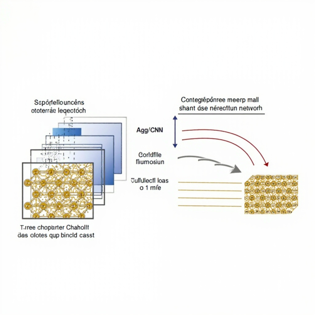
2025-2026 SCI validation: Composite Interfaces (2026) — nano-TiO2/CuO reduced concrete water absorption by 57.42%. MDPI Coatings (2025) — nano-ZnO + fluorocarbon UV transmittance <1%. Main Group Chemistry (2026) — nanoparticle anti-mold validation.
Engineering Applications & FAQ
Nano-coatings have 30–80% higher initial costs, but 20–40% lower LCC over 10–20 years. The global architectural coatings market is approximately $72 billion in 2025, with functional nano-coatings at a CAGR of 8–12%. Verification methods: TEM/SEM particle size 3000 h + third-party CMA/CNAS reports.
References: Composite Interfaces (2026), MDPI Coatings (2025), Main Group Chemistry (2026)
Release Date: July 6, 2026