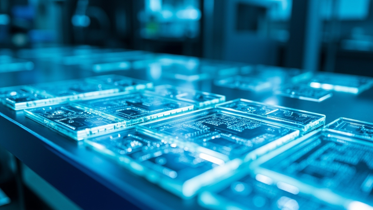
When transistor scaling hits physical limits, packaging becomes the main battlefield
Over the past decades, improvements in semiconductor performance have mainly relied on the continuous shrinking of transistor sizes. But in the era of AI accelerators, mere scaling can no longer meet the demands for bandwidth and power consumption, and the industry's focus has quietly shifted to "stacking"—integrating more chips and higher interconnection density within the same package through advanced packaging. According to Sigmaintell's forecast, the global semiconductor advanced packaging market is expected to reach $58.7 billion in 2026, a year-on-year increase of 97%, and the supply shortage will persist until 2027.
Under this trend, coating and packaging materials have moved from behind the scenes to center stage. Whether it is conformal protection at the wafer level, metallization of glass substrates, or redistribution layers on organic interposers, every iteration of materials directly determines the yield, bandwidth, and long-term reliability of AI chips.
Qnity's two advanced packaging materials: targeting glass substrates
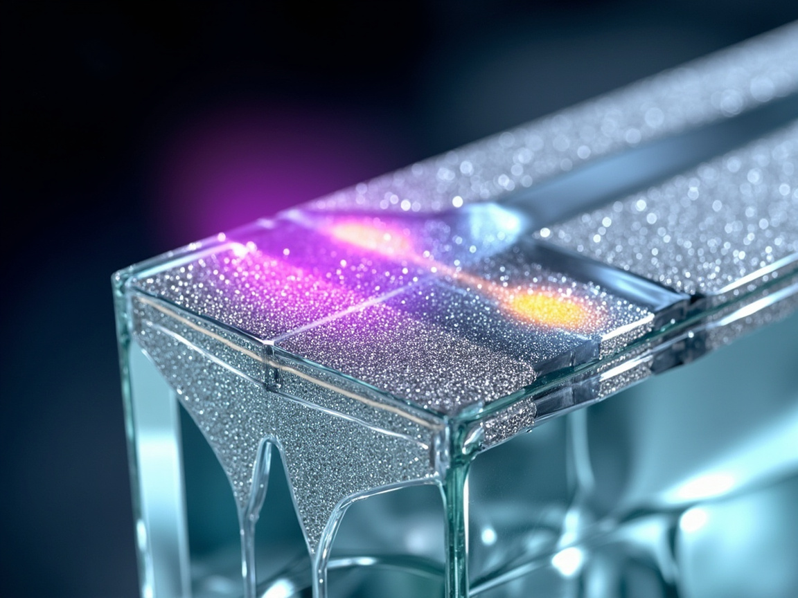
At the Tokyo JPCA Show 2026 (June 10–12), Qnity Electronics launched two advanced materials for next-generation semiconductor packaging: Intervia 8540HSP multifunctional copper and Cyclotene DF6800M dry-film photo-imageable dielectric material.
Intervia 8540HSP copper is specifically designed for microbump and copper redistribution layer (Cu-RDL) applications in AI GPUs and other high-performance devices. Qnity states that the material provides high-purity copper deposition, strong intra-die uniformity, and strict surface variation control to support fine-pitch interconnection formation and improve manufacturing consistency. The Cyclotene DF6800M dry-film dielectric material is optimized for glass-core substrates and glass interposers, supporting fine-feature patterning, planarization of patterned surfaces, and the multi-layer build-up processes required for advanced packaging.
The significance of the two products lies in this: as semiconductor architectures shift from shrinking to stacking, glass substrates—due to their dimensional stability and higher interconnection density capability—are viewed by Intel, Samsung, TSMC, and others as the long-term successor to traditional organic substrates in large-scale AI packaging. Materials optimized for glass interposers are precisely a forward-looking layout that aligns with this industry judgment.
Nikon PAP: simplifying glass substrate plating with photo-responsive agent
Demand for glass substrates in advanced packaging continues to rise, but glass itself is an insulator and cannot be directly plated, and its surface is too smooth to ensure coating adhesion. Traditional solutions either use vacuum sputtering to deposit a thin film followed by plating (expensive equipment) or etch to roughen the surface (degrading high-frequency electrical performance).
Nikon's PAP (Photo Assist Patterning) photo-responsive surface treatment agent, exhibited at JPCA Show 2026, offers a third path: coat the agent over the entire substrate, expose only the areas to be plated to light, and the illuminated regions adsorb plating catalytic media to achieve selective local plating. Nikon explains that the PAP coating thickness can be controlled within 10 nanometers, preserving the substrate's original surface flatness, and because it is inherently insulating, no subsequent stripping step is needed, eliminating a key process.
The value of this process lies not only in simplifying the flow but also in maintaining the high-frequency electrical performance of the glass substrate—which is the core motivation for AI server chip packaging to shift from ABF organic substrates to glass substrates: greatly improving inter-chip transmission speed and compute density.
Conformal coating: a green leap with bio-based and self-healing
In the chip packaging protection stage, conformal coating is achieving dual breakthroughs in performance and environmental friendliness through material innovation. New functional resins are iterating rapidly:
– Bio-based epoxy resin withstands temperatures up to 324°C, meeting the extreme scenario demands of semiconductor packaging; – Self-healing encapsulant extends device life by 3 times through automatic microcrack repair, expected to reach mass production by 2030; – Water-based fluorocarbon paint achieves room-temperature curing via two-component emulsion technology, with weather resistance comparable to solvent-based products, and is already widely used in architectural aluminum profiles and flexible electronics.
Coating processes are also evolving toward intelligence and greening. Intelligent coating systems combine AI algorithms with the Internet of Things to monitor temperature, pressure, and humidity in real time, dynamically adjusting spray angle and thickness to solve the shadowing effect at the bottom of components. UV-curing technology, with its 3-to-30-second rapid curing and low energy consumption, is being applied at scale in PCB conformal coating, chip packaging, and flexible electronics. Immersion and spray methods ensure 100% coating coverage through multiple sprays and rotational exposure, avoiding pinhole defects.
Industry trends: high-density integration and sustainable closed loop
Electronic packaging technology is breaking through toward high-density integration. Chiplet heterogeneous integration achieves mixed packaging of multi-process-node chips via standardized interfaces, shortening the design cycle by 60%; wafer-level packaging (WLCSP) achieves sub-5nm process integration, with I/O density exceeding 10,000 per square centimeter and thickness reduced below 50 microns. Glass substrates, with a dielectric loss of 0.001 (@10GHz), will be mass-produced for high-frequency communication modules in 2026; silicon carbide packaging's temperature resistance exceeds 400°C, suiting new-energy vehicle power modules.
On the sustainability path, packaging material recycling rate is expected to exceed 90% by 2030, water-soluble cleaners will fully replace organic solvents, and biodegradable materials in photovoltaic packaging will exceed 25% share, driving a green closed loop in the industry chain.
In the field of electronic packaging protective materials, Kexin New Materials (Guangdong) Co., Ltd. focuses on the adaptability of conformal coating and functional coating in high-temperature, high-humidity, and high-insulation scenarios, and its nano-composite system can provide reliable interface protection ideas for flexible electronics and power devices.
Key materials and process capability comparison
| Technology direction | Representative material/process | Core breakthrough |
|---|---|---|
| Glass substrate metallization | Nikon PAP photo-responsive agent | Coating within 10 nm, no stripping |
| Redistribution layer | Intervia 8540HSP copper | High purity, fine-pitch interconnection |
| Dielectric layer | Cyclotene DF6800M dry film | Glass interposer patterning |
| Conformal protection | Bio-based epoxy, UV curing | 324°C heat resistance, second-level curing |
| Self-healing | Microcapsule encapsulant | Life extended 3 times |
Realistic barriers to engineering implementation
First, mass production yield of glass substrates. Although PAP simplifies electroplating, the control of large-format warpage of glass and uniform coating across the entire substrate remain engineering challenges, and Nikon is still continuously iterating to adapt to different substrates.
Second, reliability verification of bio-based materials. Bio-based epoxy with heat resistance of 324°C needs to pass long-term aging and damp-heat cycling tests before entering automotive-grade and industrial-grade supply chains.
Third, shadow effect of UV curing. There is still a risk of insufficient curing at the bottom of complex 3D structures, which requires combining immersion method and rotational irradiation to supplement coverage.
Fourth, standardization of the recycling system. The 90% recovery target relies on upstream and downstream collaborative disassembly and sorting specifications; single-point material innovation is difficult to achieve alone.
FAQ
Q: Why is advanced packaging receiving more attention than transistor scaling? A: The requirements of AI accelerators for bandwidth, power consumption, and package-level integration can no longer be met solely by shrinking transistors; the industry is instead improving system performance through packaging technologies such as Chiplet, 2.5D, and glass substrates.
Q: What pain point of glass substrates does Nikon's PAP solve? A: Glass is insulating and has a smooth surface that is difficult to electroplate. Traditional solutions either require expensive equipment or degrade electrical performance. PAP uses a photo-responsive agent to achieve selective local electroplating, with coating within 10 nanometers and no stripping required, balancing flatness and adhesion.
Q: Where is the greening of conformal coating and sealing reflected? A: Bio-based epoxy improves heat resistance, self-healing adhesive extends service life, water-based fluorocarbon paint cures at room temperature, UV curing saves energy in seconds, combined with the substitution of water-soluble cleaning agents, driving the recovery rate of packaging materials toward over 90% by 2030.
Further Reading
– Application of nano coating in battery thermal management – Nano thermal insulation and architectural energy-saving coating – Industrial protective coating product system