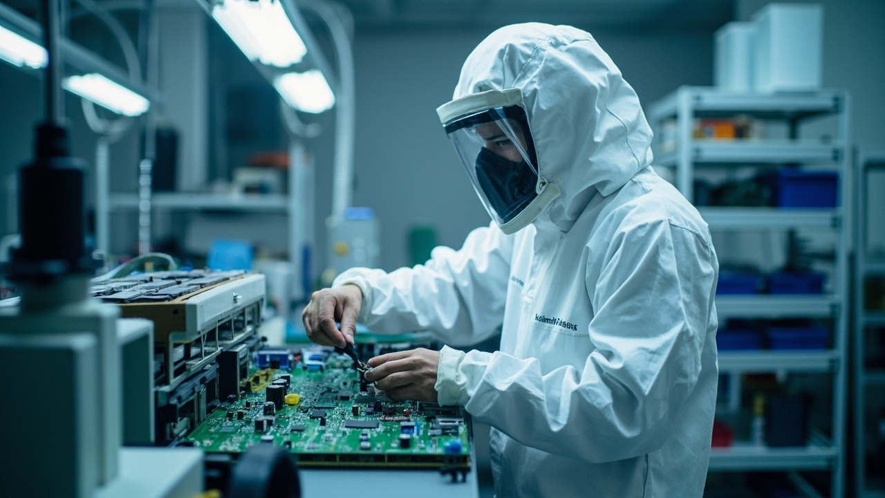
Today, with smart terminals, automotive electronics, wearable devices, and industrial IoT sensors being widely adopted, electronic device failures increasingly no longer originate from the chip itself, but from the "environment"—moisture, salt spray, condensation, dust, and electrochemical migration silently erode circuits at the microscopic scale. Traditional PCB conformal coating can extend service life from "a few months" to "several years," but as devices become further miniaturized, flexible, and high-frequency (5G/mmWave/RF), more demanding requirements are placed on the protective layer: it must be superhydrophobic and liquid-repellent, have high volume resistivity insulation, and be as thin as possible without affecting signal and heat dissipation. This contradiction is exactly the backdrop for the emergence of nano protective coating for electronic devices—especially aerogel ceramic composite coating.
As a company focused on R&D and industrialization of functional coatings, kexin new materials (kexinMaterials) has accumulated extensive formulation and process data on superhydrophobic insulating nano coatings and aerogel composite ceramic systems. This article will also combine public standards (IPC-CC-830, IEC 61086, UL 746E, etc.) with real TDS data to systematically break down the technical logic of nano protective coating for electronic devices, helping engineers "speak with data" during selection and acceptance.
I. Why electronic devices need nano-scale protection
The failure mechanism of electronic equipment is essentially a "micro-electrochemical" process. When moisture or conductive contaminants (salt spray, sweat residue, flux ions) adhere to the PCB surface, a miniature electrochemical cell forms between adjacent conductors: anode metal dissolves, ions migrate in the liquid film, and cathode reduction occurs, ultimately manifesting as increased leakage current, dendrite growth (electrochemical migration, ECM), and even short circuits between adjacent traces. The internationally recognized conformal coating standard IPC-CC-830 (the successor and replacement of the former US military specification MIL-I-46058C) was born to break this chain, solidifying the qualification and performance testing of "electrical insulating compounds" into a unified threshold.
The core difference between nano protective coating and traditional conformal coating lies in "scale":
- Thinner film, better conformality: Traditional conformal coating typically has a film thickness of 25–250 µm (IPC-CC-830 commonly 25–75 µm), while some nano ceramic coatings can reach 80–400 nm level, offering stronger "topographical conformality" to miniature components, connector pins, and MEMS microstructures;
- Lower surface energy, more thorough hydrophobicity: By combining micro-nano rough structures with low-surface-energy chemical groups, the water contact angle can be pushed into the superhydrophobic range;
- Composite functionality: Combining aerogel (extremely low dielectric constant, extremely low thermal conductivity), ceramic (high hardness, insulation, temperature resistance) with hydrophobic groups achieves the superposition of "insulation + liquid repellency + temperature resistance + lightweight".
Key conclusion: Nano protective coating for electronic devices is not simply making conformal coating "thinner," but reconstructing surface energy, dielectric, and thermal behavior at the nm scale.

II. Superhydrophobic insulation: contact angle, roll-off angle, and leakage suppression mechanism
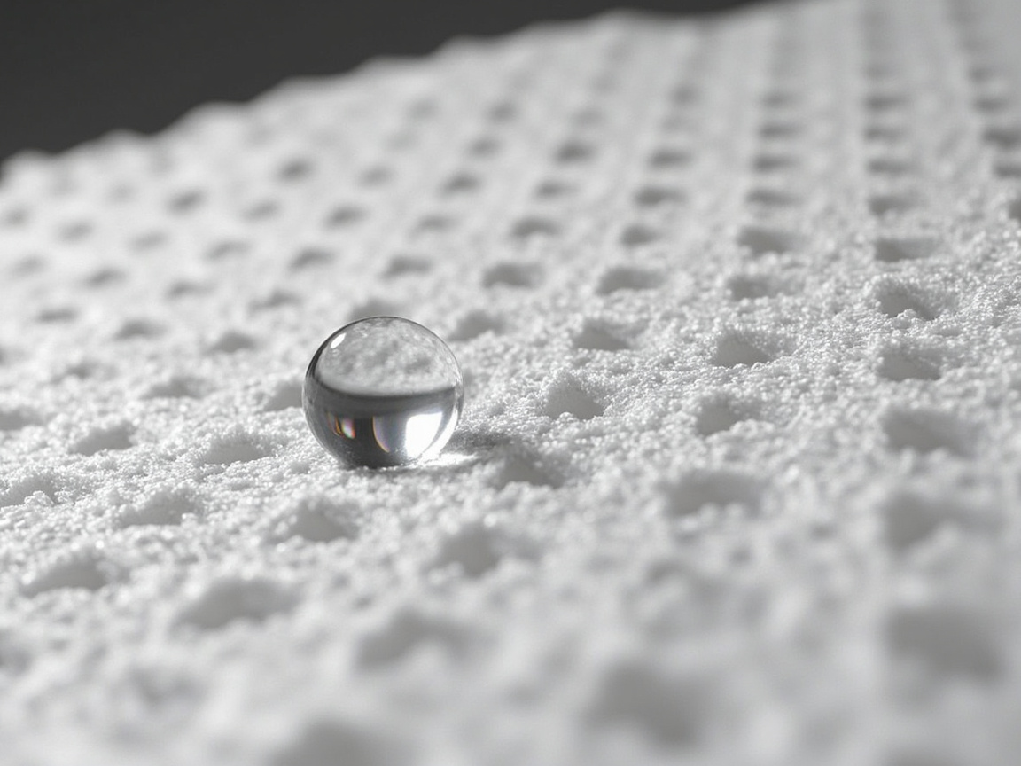
"Superhydrophobic" is academically defined as water contact angle (CA) >150°, roll-off angle (SA) <10°—water droplets are nearly spherical and roll off with a slight tilt, without spreading into a continuous liquid film. For electronic devices, this directly cuts off the physical premise of "liquid film bridging conductors," which is a geometric means to suppress leakage and electrochemical migration from the source.
Its mechanism comes from the superposition of two things (Wenzel and Cassie–Baxter models):
- Micro-nano binary rough structure: Nanoparticles (such as SiO₂, ceramic particles) build micro-nano level bumps on the surface, "locking" air in the pores of the rough structure, so that water droplets actually only contact a few solid vertices;
- Low-surface-energy chemical modification: Through silanization and other treatments, hydrophilic silanol groups are converted to hydrophobic methyl/fluoroalkyl groups (note: electronic protective coating needs to balance subsequent repairability and RoHS, often favoring fluorine-free or low-fluorine routes).
It must be emphasized that superhydrophobic does not equal "high insulation"; the two are indicators of different dimensions: hydrophobicity solves "whether a liquid film forms," while insulation solves "whether leakage current is controllable even with trace moisture." Therefore, electronic protective coating must simultaneously meet the two hard indicators of hydrophobicity and high resistivity.
Engineering tip: Once the superhydrophobic surface is damaged by oil, dust, or repeated friction destroying the microstructure, it may "degrade from superhydrophobic to high adhesion," making it easier to retain liquid. Therefore, wear resistance and adhesion are mandatory inspection items for electronic nano coatings, not optional.
III. Aerogel ceramic composite coating: dual benefits of ultra-low dielectric constant and thermal insulation
Among nano protective coatings for electronic devices, a noteworthy direction is the aerogel + nano ceramic composite system. According to silica aerogel review literature indexed by ScienceDirect, silica aerogel has the following intrinsic properties, making it an ideal functional filler for electronic protection:
- Ultra-high porosity: Porosity typically >90% (literature reports 80%–99.8%), pore size mostly 1–100 nm;
- Ultra-high specific surface area: 500–1200 m²/g;
- Extremely low thermal conductivity: At room temperature and pressure about 0.012–0.025 W/(m·K), about 1/3 of still air, one of the known solid materials with the lowest thermal conductivity ("super insulation");
- Ultra-low dielectric constant: k value about 1.0–2.0, far lower than conventional polymers (generally 2.5–3.5 or above);
- Inorganic, non-combustible/flame-retardant, good chemical inertness;
- After hydrophobic modification, water contact angle can reach 109.9°–130.0°.
Mapping these to electronic protection, the value is very direct:
| Intrinsic property of aerogel | Engineering significance for electronic devices |
|---|---|
| Ultra-low dielectric constant k=1.0–2.0 | Reduce high-frequency/RF signal loss and crosstalk, suitable for 5G, mmWave, antenna area protection |
| Extremely low thermal conductivity 0.012–0.025 W/(m·K) | Slow local thermal shock, protect temperature-sensitive miniature components |
| Porosity >90%, ultra-light | Almost no weight increase, suitable for wearable/portable devices |
| Inorganic non-combustible | Improve fire safety, aligned with UL 94 philosophy |
| Hydrophobic modified CA up to 130° | Assist in achieving superhydrophobic liquid-repellent surface |
A real product form reference comes from public TDS data: ECS 1300AG electronic superhydrophobic insulating nano ceramic coating, a single-component system composed of aerogel particles + nano ceramic, film thickness 12–25 µm, featuring superhydrophobicity, electrical insulation, extremely strong anti-corrosion and good adhesion; fluorine-free polymer, silicon-free; compliant with RoHS / REACH / WEEE; can be applied by spraying, wiping, or dipping, cured at room temperature in air (can be heated to accelerate), mainly single pass. Its labeled application objects cover PCB, consumer electronics, wearables, optical devices, micro-motors, connectors, and sensors, and after curing it is inert, odorless, smoke-free, and eco-friendly.
The technical point here is: aerogel contributes "low-k dielectric + thermal insulation + lightweight," nano ceramic contributes "insulation + hardness + temperature resistance + wear resistance," and after composite they are implemented with a single-component room-temperature curing process, exactly matching the electronics industry's demands for "low energy consumption, thin coating, compliance."
IV. PCB conformal coating standards and electrical indicators (core data table)
Whether using traditional conformal coating or nano protective coating, acceptance should return to standards and quantifiable indicators. Key standards in electronic protection include:
- IPC-CC-830: Qualification and performance standard for electrical insulating compounds for printed board assemblies (replacing MIL-I-46058C), specifying dielectric withstand, humid insulation, thermal shock, flame retardancy tests;
- IEC 61086: International standard for coating materials for electronic assemblies;
- UL 746E: Safety standard for polymer materials for electrical equipment (flame retardancy per UL 94, preferably V-0/V-1);
- IPC-A-610: Acceptability (appearance/coverage/defects) criteria for assembled boards;
- J-STD-001: Soldering requirements prior to coating;
- ASTM D257: DC resistance/conductance of insulating materials (volume resistivity, surface resistivity) test;
- ASTM D149: Dielectric strength (breakdown voltage) test;
- GB/T 31838: Domestic counterpart standard for volume resistivity and surface resistivity of solid insulating materials.
According to public industry technical references (e.g., overview of high-insulation conformal coating specifications), the key electrical metrics for quality high-insulation protective coatings are approximately:
| Metric | Typical magnitude | Test standard / note |
|---|---|---|
| Volume resistivity | ≥10¹⁴ Ω·cm | ASTM D257 / GB/T 31838 |
| Surface resistivity | ≥10¹² Ω | ASTM D257 / GB/T 31838 |
| Dielectric strength (breakdown voltage) | 25–40 kV/mm | ASTM D149 |
| Dielectric constant | 2.5–3.5 (lower is more favorable for high frequency) | Concern in high-frequency scenarios |
| Loss factor tanδ | <0.01 (more sensitive for RF/microwave) | Affects signal integrity |
| Dielectric Withstand Voltage (DWV) | ≥1500 V AC / 60s no breakdown | IPC-CC-830 requirement |
| Moisture Insulation Resistance (MIR) | 85℃/85%RH 7 days, insulation >100 MΩ | IPC-CC-830 requirement |
| Thermal shock | -65℃↔+125℃, 10 cycles no cracking/no delamination | IPC-CC-830 requirement |
| Salt spray resistance | After 1000 h neutral salt spray, insulation attenuation <1 order of magnitude | Reference ASTM B117 |
Note: The "Typical magnitude" in the table above represents the high-insulation product range given in public industry overviews, not a committed value for any specific model; specific selection must be based on the supplier's third-party test report. When using nano aerogel ceramic coating, its low-k dielectric constant (k=1.0–2.0) may actually outperform traditional conformal coatings in RF and high-speed signal scenarios.
V. Film Thickness Design and Inspection (nm–µm scale)
There is a "golden range" for the film thickness of electronic protective coatings: too thin, and the moisture barrier is insufficient; too thick, it not only affects component heat dissipation but may also crack under thermal cycling. According to IPC-CC-830 and industry practice, the recommended dry film thickness for conformal coatings is 25–75 µm; below 25 µm protection drops significantly, and above 100 µm the risks of thermal cycling cracking and heat dissipation rise. Nano ceramic coatings, due to different mechanisms, can go down to nm scale—for example, the aforementioned ECS 1300AG is 12–25 µm, and some automotive-grade/glass-ceramic nano coatings can achieve 80–400 nm.
Different thickness scales require matching measurement methods:
| Thickness range | Typical method | Application scenario |
|---|---|---|
| 1–1000 nm | Ellipsometer (Spectroscopic Ellipsometry) | Nano ceramic, thin film, wafer-level coating |
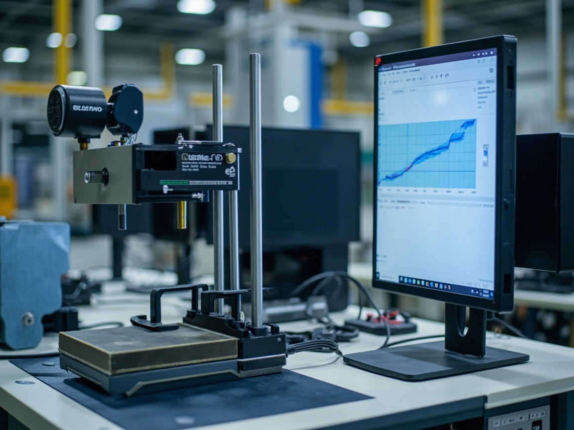
| Tens of nm–hundreds of µm | Stylus Profilometry / Surface Profiler | Nano coating cross-section, film thickness step |
| nm–µm | SEM cross-section observation | Micro-morphology and interface |
| 25–250 µm | Eddy current thickness / Cross-section method | PCB conformal coating (IPC-CC-830 recommends 5–10 points/board) |
Under different deposition processes, film thickness ranges also follow patterns (based on review of nano composite coating deposition research):
- Spray: approx. 5–100 µm, suitable for complex 3D geometry but with edge buildup;
- Dip: approx. 1–50 µm, high material utilization but thinner at top end;
- Spin: approx. 0.1–10 µm, best uniformity but limited to planar surfaces.
For electronic devices, film thickness is not "the thicker the safer". A balance should be struck between "reaching insulation/hydrophobic threshold" and "not sacrificing heat dissipation/flexibility", and multi-point actual measurement should replace visual inspection.
VI. Application Process: Surface Cleaning, Coating and Curing Window
For electronic protective coatings, "seven tenths lies in surface treatment". Even with the best formulation, flux residue, oil, and silicone oil on the substrate will cause cratering and loss of adhesion. The common industry practice (refer to IPC cleaning specification) is:
- Cleaning: Use isopropanol (IPA) or dedicated cleaning agent to remove flux residue, rinse with DI water if necessary, and verify ionic cleanliness;
- Surface energy assessment: Many coatings require substrate surface energy >38 dyne/cm, which can be quickly screened with a dyne pen;
- Coating: Single-component systems like ECS 1300AG support spray/wipe/dip, mainly single pass; for complex boards, selective coating is recommended to avoid connectors and test points;
- Curing: Ambient air curing is sufficient, can be accelerated by heating; inert after curing. A process window of "avoid water/dust" must be reserved to prevent contamination before curing.
For aerogel ceramic coatings, flexibility must also be considered in engineering—rigid coatings may crack on flexible PCBs or under large ΔT conditions; if necessary, a more flexible formulation or reduced film thickness should be selected, which follows the same logic as traditional conformal coatings' "switch to silicone for thermal cycling cracking".
VII. Selection Decision and Supporting Recommendations
Turn the above logic into an executable selection framework:
- High-frequency/RF/antenna areas: Prioritize low dielectric constant systems (aerogel composite, k≈1.0–2.0) to avoid signal loss;
- High humidity/salt spray outdoor (e.g., automotive ECU, outdoor sensors): Superhydrophobic + high volume resistivity both qualified, and third-party salt spray report required;
- Wearable/portable: Lightweight, thin coating, flexibility first; aerogel's "almost no weight gain" is an advantage;
- Repairable consumer electronics: Focus on removability, fluorine-free/low-fluorine and RoHS/REACH compliance.
In this direction, kexinMaterials can provide a complete solution from aerogel ceramic nano coating formulation, surface treatment process cards to third-party testing coordination, helping customers stably reproduce "superhydrophobic + insulation + compliance" on the production line. If your working conditions involve both corrosive media and protective coating, you may also refer to our article on barrier and corrosion inhibition enhancement of nano composite anti-corrosion coating to understand how nano flakes extend the corrosion path; for the specific definition of hydrophobic characterization, you can further read nano coating hydrophobic angle and sliding angle.
VIII. Common Selection Misconceptions
Misconception 1: Superhydrophobic = high insulation. Wrong. Hydrophobicity only solves whether a liquid film forms; insulation depends on volume resistivity and dielectric strength, both of which must be verified separately.
Misconception 2: Thicker film is safer. Wrong. Excessive thickness sacrifices heat dissipation and increases thermal cycling cracking risk; IPC-CC-830 recommends 25–75 µm, and nano coatings also need a lower limit set by mechanism rather than blindly thickening.
Misconception 3: Nano coatings need no standards. Wrong. Electronic protection should still return to existing standards such as IPC-CC-830, IEC 61086, UL 746E, etc. So-called "nano" is not an excuse to exempt testing; rather, due to scale effects, agglomeration and uniformity must be strictly controlled.
Misconception 4: Only look at advertised contact angle values. Wrong. One should also look at sliding angle, contact angle retention after abrasion, and insulation attenuation after salt spray; a single metric is easily packaged.
Misconception 5: Because nano coatings are "thin", the lower film thickness limit can be ignored. Wrong. Although nano systems can reach nm scale, protection (hydrophobic/insulation/anti-corrosion) still has an effective dense layer thickness threshold; below it, local pinholes will "short-circuit" the protection of the entire board. Thin is a means, not an end; the lower film thickness limit must be held according to mechanism and standards.
IX. Volume Resistivity and Surface Resistivity: What Is the Engineering Difference
When accepting electronic protective coatings, engineers often treat "insulation" as a vague indicator, but in fact it can be broken down into at least two measurable dimensions (both per ASTM D257 / domestic GB/T 31838, using the three-electrode method):
- Volume resistivity (ρv, unit Ω·cm): measures the material's ability to internally block leakage current, closer to the intrinsic insulating property of the coating; high-insulation products typically require ≥10¹⁴ Ω·cm.
- Surface resistivity (ρs, unit Ω/□): measures the ability of leakage along the surface, greatly affected by ambient humidity, surface contamination, and condensation; high-insulation products typically require ≥10¹² Ω.
The engineering significance of the two differs: superhydrophobic coatings mainly improve "surface liquid repellency", thereby indirectly stabilizing surface resistivity—because once a water film spreads, ρs drops precipitously; while volume resistivity is determined by the intrinsic structure of ceramic/airgel, and is relatively less affected by moisture. Therefore, a robust electronic protection scheme should be a double insurance of "superhydrophobic secures the surface + high ρv holds the interior".
In practice, one must also look at the decay after damp heat: according to a review of high-insulation conformal coating indicators, a qualified protective coating after 1000 hours at 85℃/85%RH should have insulation resistance decay of less than one order of magnitude (i.e., still maintaining the same order of high resistance value), rather than "insulating when dry, leaking when wet".
X. Application Segmentation: Automotive Electronics, Wearables, Medical and Aerospace
Different application scenarios have significantly different focuses on nano protective coatings, and should be treated separately during selection:
- Automotive electronics (ECU, sensors, headlights, charging pile modules): simultaneously facing high humidity, salt spray, vibration, and temperature cycling. Referring to public TDS, automotive-grade nano ceramic coatings can cover -45℃~180℃ (e.g., Re-yingcai YCC05006G, neutral salt spray ≥1200 h), which is especially critical for engine compartment periphery and onboard connectors.
- Wearable devices (watches, earphones, medical patches): long-term contact with sweat (salty), frequent bending. The "almost no weight gain" and flexible adaptation of airgel ceramic coatings are advantages; meanwhile, fluorine-free/low-fluorine and RoHS/REACH compliance should be prioritized for skin contact safety.
- Medical electronics: stringent requirements for biocompatibility and low migration. In industry cases, implantable or long-term body-fluid-contact devices often use parylene (Parylene C, ISO 10993 biocompatible) or equivalent inert coatings; if a nano ceramic system enters this field, it must provide corresponding biocompatibility and extraction evaluation, rather than just looking at insulation numbers.
- Aerospace and extreme outdoor: facing special tests such as wide temperature variation, irradiation, and vacuum outgassing. The ultra-low thermal conductivity (0.012–0.025 W/(m·K)) and ultra-low dielectric constant (k=1.0–2.0) of airgel are valuable in thermal management and high-frequency links, but the space environment also requires additional verification of irradiation stability and vacuum degassing. This article does not expand on specific values, only noting "ground standard ≠ space qualification".
- Industrial IoT sensors: long-term outdoor exposure. According to public engineering cases (e.g., outdoor environmental sensors using silicone dip coating 75–100 µm, room temperature 48 h curing), MTBF can be increased from about 18 months to about 7 years—this confirms the core value that "protective coating pulls lifespan from months to years", and the nano system further reduces film thickness and signal loss to lower levels.
For quick decision-making, an application–indicator quick-reference matrix is given:
| Application scenario | Primary demand | Recommended coating property |
|---|---|---|
| Automotive ECU/connector | Salt spray resistance, temperature variation resistance | Superhydrophobic + high ρv + temperature resistance -45~180℃ |
| Wearable | Lightweight, flexible, compliant | Airgel composite, fluorine-free, RoHS/REACH |
| RF/antenna | Low signal loss | Low-k (airgel k=1.0–2.0) |
| Medical electronics | Biocompatible, low migration | Inert/ISO 10993 evaluation |
| Industrial IoT | Long life, maintenance-free | Superhydrophobic + thick film durability |
XI. Acceptance Checklist and Implementation Cooperation
Turning the aforementioned points into an executable offline acceptance checklist is more reliable than any slogan:
- Surface cleanliness and surface energy: remove flux/oil, surface energy >38 dyne/cm;
- Multi-point film thickness measurement: ellipsometry/step profiler/eddy current selected by scale, 5–10 points per board;
- Hydrophobic characterization: contact angle + rolling angle, and measure retention after abrasion;
- Electrical indicators: volume resistivity (≥10¹⁴ Ω·cm), surface resistivity (≥10¹² Ω), dielectric strength (25–40 kV/mm), dielectric withstand (≥1500 V AC/60s);
- Environmental reliability: neutral salt spray 1000 h, insulation decay after 85/85 damp heat <1 order of magnitude;
- Adhesion and curing degree: cross-cut (refer to GB/T 9286 / ASTM D3359), FTIR to confirm sufficient curing.
When importing the above checklist into the mass production line, Kexin New Materials (kexinMaterials) can provide packaged support of "formula + process card + third-party testing interface", helping customers achieve stable balance among superhydrophobicity, electrical insulation, and compliance, rather than leaving risks for on-site rework. For how nano-platelets further extend the corrosion path, you can read the extended article Nano Composite Anti-corrosion Coating: Barrier and Corrosion Inhibition Enhancement, which together with the electrical protection of this article forms a "anti-corrosion + insulation" dual-dimensional coverage.
XII. Significance of Airgel Low Dielectric Constant for 5G/RF Links
When discussing electronic protective coatings, engineers often only focus on "is the insulation enough", but ignore the impact of the protective layer itself on high-frequency signals. When the coating covers near antennas, RF front-ends, or high-speed traces, its dielectric constant (k) participates in the boundary conditions of the electromagnetic field: the higher the k, the "heavier" the effective dielectric environment for signal propagation, and the more likely to introduce insertion loss, phase shift, and impedance mismatch.
The key comparison comes from real data: according to a review of high-insulation conformal coating indicators, traditional high-insulation protective coatings have dielectric constants mostly in 2.5–3.5; while the intrinsic dielectric constant of silica airgel is only k=1.0–2.0 (ScienceDirect review). This means that airgel ceramic composite coatings, while providing superhydrophobicity and insulation, disturb the electrical performance of 5G, millimeter wave, antenna, and RF links significantly less—in scenarios where "protection is needed but signal must not be dragged down", this is its differentiated value relative to traditional conformal coatings.
What needs to be balanced is the thermal side: the thermal conductivity of airgel is only 0.012–0.025 W/(m·K), which is an excellent "thermal buffer" but not "efficient heat dissipation". For heating devices, one should not rely on the protective layer for heat conduction, but position it as a role of "local thermal insulation protection + low signal disturbance", with heat dissipation still relying on the metallization of the device body and heat dissipation channel design. In short, the correct positioning of airgel ceramic coatings in electronics is "low-k dielectric shield", not "thermal conductive layer".
In engineering acceptance, the dielectric constant itself also needs to be measured rather than assumed constant: the effective k value of the coating can be measured at the target frequency band by parallel plate capacitance method or resonant cavity method to confirm it falls in the expected low-k range; for RF/antenna areas, it is recommended to compare insertion loss and return loss on the assembled whole machine or module, turning "protection does not drag down signal" from concept into a recordable data point.
FAQ
1. What is the difference between electronic device nano protective coating and traditional PCB conformal coating?
Traditional conformal coatings (acrylic/polyurethane/silicone/epoxy/parylene) mostly have film thickness of 25–250 µm, using "covering" to block moisture and dust; nano protective coatings (especially airgel ceramic types) can be made thinner (e.g., 12–25 µm or even nm level), and have advantages in low dielectric constant, lightweight, and superhydrophobic fitting to microstructures. The two are not a substitution relationship, but complementary according to device scale and frequency band requirements.
2. What is superhydrophobic, and why do electronic protections need it?
Academically, superhydrophobic means water contact angle >150°, rolling angle <10°, water droplets are spherical and easy to roll off, difficult to spread into a continuous liquid film on the circuit board surface, thereby cutting off the liquid film bridging and electrochemical migration between adjacent conductors from the source. But it cannot replace high-insulation indicators, and must simultaneously meet volume resistivity and dielectric strength.
3. What special benefits does airgel coating have for electronics?
Silica airgel has porosity >90%, thermal conductivity 0.012–0.025 W/(m·K), dielectric constant k=1.0–2.0, and is inorganic and non-combustible. For electronics, low-k means low high-frequency/RF signal loss and low crosstalk; extremely low thermal conductivity can buffer thermal shock; ultra-light almost no weight gain, very suitable for wearables and portable devices.
4. What are the key electrical indicators for PCB protective coatings, and what standards to refer to?
Core indicators include volume resistivity (≥10¹⁴ Ω·cm, ASTM D257/GB/T 31838), dielectric strength (25–40 kV/mm, ASTM D149), dielectric withstand voltage (≥1500 V AC/60s, IPC-CC-830), damp heat insulation (85℃/85%RH 7 days >100 MΩ), thermal shock (-65℃↔+125℃), etc.; standards mainly refer to IPC-CC-830, IEC 61086, UL 746E.
5. How thick should the electronic nano coating film be?
Depends on the system: traditional conformal coating IPC-CC-830 recommends 25–75 µm; below 25 µm protection is insufficient, and above 100 µm it is prone to cracking and hinders heat dissipation; nano ceramic coating can be as low as 12–25 µm or at the nm level (e.g., 80–400 nm), but all must be governed by the principle of "achieving the hydrophobic/insulation threshold without affecting heat dissipation and flexibility", and measured with an ellipsometer/step profiler.6. What is the biggest pitfall in nano coating construction?
Surface cleaning. Flux residue, oil, and silicone oil can cause cratering and loss of adhesion; they must be removed according to IPC cleaning specifications and the surface energy verified (>38 dyne/cm). In addition, a curing water-avoidance window should be reserved to prevent contamination of the uncured coating.
7. Is aerogel coating flame retardant, and what should be noted for compliance?
Silica aerogel is an inorganic material and is generally non-combustible/flame retardant; electronic-grade systems also need to address compliance such as RoHS, REACH, WEEE, and prioritize fluorine-free or low-fluorine routes to facilitate rework and environmental protection. The specific compliance status is subject to the product TDS and test reports.
8. Can rigid nano ceramic coating be used on flexible circuit boards?
Use with caution. Rigid coatings may crack under large thermal cycles or bending; for flexible PCBs, it is recommended to use a more flexible formulation, reduce film thickness, or adjust the system by referring to the idea of "switch to silicone when thermal cycling causes cracking".
9. Is it normal for insulation resistance to drop after humidity-heat exposure?
It should not drop significantly. A qualified high-insulation protective coating should show an insulation resistance attenuation of less than one order of magnitude after 1000 hours at 85℃/85%RH; if the resistance drops cliff-edge style after humidity-heat, it often indicates hydrophobic failure, presence of pinholes, or intrinsically insufficient volume resistivity, requiring a review of surface treatment and formulation.
10. Can nano coatings be used in medical or food-contact electronics?
Yes, but the threshold is higher. In addition to electrical and hydrophobic metrics, biocompatibility (e.g., ISO 10993) and low extraction/low migration evaluation are required, and compliance such as RoHS/REACH must be confirmed. If an aerogel ceramic system enters such scenarios, corresponding safety and extraction data must be provided, rather than using "nano" "ceramic" merely as a safety endorsement.
Further Reading
- Nano Coating Hydrophobic Angle and Rolling Angle: Characterization and Self-Cleaning Significance: supplements the contact angle/rolling angle definitions and test methods behind "superhydrophobic" in this article.
- Nano Coating Film Formation and Curing: Room Temperature/IR/Baking and Thickness (nm–µm): understand the ambient air curing mechanism and film thickness control logic of aerogel ceramic coatings.
- Nano Composite Anti-Corrosion Coating: Barrier and Corrosion Inhibition Enhancement: when electronic devices are also exposed to corrosive media, learn how nano platelets extend the corrosion path.