The reason nano coatings are "thin yet strong" lies fundamentally in their functional layers being only at the nanometer-to-micrometer scale: for example, common SiO₂-based automotive ceramic coatings on the market have a film thickness of about 1–3 µm (per Gaamp360 technical data), while some automotive paint nano ceramic shields are only 200–400 nm thick (per Onyx Nano Shield data). Whether such a thin layer can truly deliver superhydrophobicity, hardening, scratch resistance, and corrosion resistance depends almost entirely on the application process—if the surface is not cleaned properly, even the most expensive nano coating will flake off in sheets; if applied too thick it sags, too thin it reveals the substrate; if the curing window misses the temperature and humidity, curing is incomplete and both contact angle and durability are greatly reduced. This article breaks nano coating application into three checkpoints—"surface treatment—application—curing"—and provides actionable parameters and criteria for each.
As a supplier of industrial and automotive coating systems, Kexin New Materials (kexinMaterials) has mature solutions for nano ceramic coatings, hydrophobic protection, and supporting pretreatment agents. The process recommendations in this article also come from the accumulation of these real working conditions, and can be directly applied in combination with the sections below.
I. Why the Application Process Determines the Success or Failure of Nano Coatings
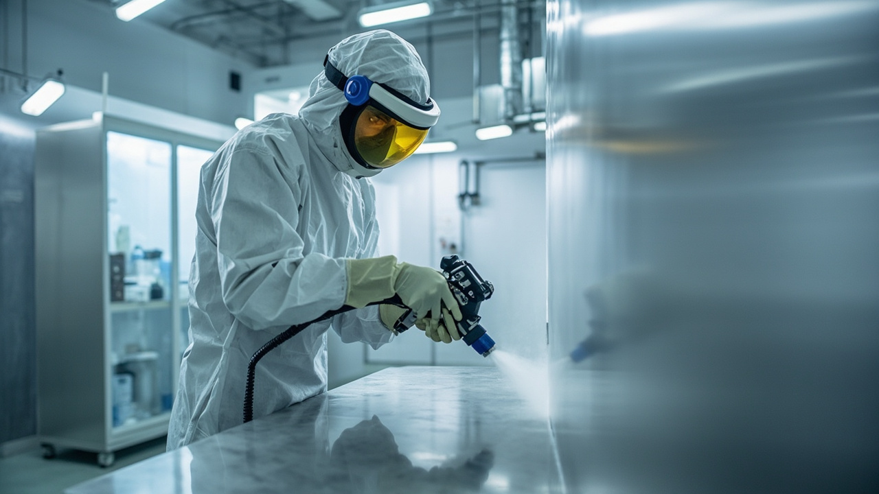
Nano coatings and traditional coatings are not even in the same league when it comes to "thickness." Traditional epoxy topcoats are often over 100 µm (e.g., a single coat of epoxy polyurethane topcoat can reach 100–120 µm, per domestic product parameter summaries), relying on thick-film physical shielding; whereas nano coatings work through surface chemistry and micro-topography—low surface energy brings a large contact angle (hydrophobicity), a dense inorganic network brings hardness and wear resistance, and the ultra-thin layer adds almost no dimension to the workpiece. The trade-off is: it is extremely sensitive to the condition of the substrate surface.
Mechanistically speaking, whether the coating can ultimately "hold on" depends on three micro-level factors:
- Mechanical anchoring: The substrate surface must have suitable micro-roughness so the coating penetrates the undulations and forms a "bite." Sandblasting to Sa 2½ (ISO 8501-1) is precisely to create such undulations.
- Chemical/physical adsorption: The substrate surface must be clean and activated, with no oil, scale, or mold release agent blocking interfacial bonding.
- Surface energy matching: According to Young's equation, cosθ = (γ_SV − γ_SL)/γ_LV, the lower the solid surface energy (γ_SV), the harder for liquid to wet it, and the larger the contact angle θ. Nano coatings themselves pursue "low surface energy," but this means they themselves are also hard to adhere to low-surface-energy plastics and waxy layers—unless activated first.
In one sentence: nano coating is "interface engineering," not "brushing on a layer of film." The three checkpoints below are broken down one by one.
II. Surface Treatment: Three Principles of Cleanliness, Roughness, and Activation
Whether it is automotive paint, electronic housings, or industrial steel structures, surface treatment accounts for the majority of application success or failure. This is especially true for nano coatings.
2.1 Degreasing and Defatting: The First Step, and the Most Easily Skipped One
Any grease, fingerprints, wax, or silicone mold release agent will form a weak boundary layer at the interface, causing the nano coating to "falsely adhere." The standard procedure for automotive ceramic coatings is to first perform IPA (isopropyl alcohol) degreasing—wipe repeatedly with IPA on non-woven cloth to remove glaze, oil, and residual polishing compounds (per Gaamp360 application process). Industrial parts commonly use alkaline degreasing, solvent wiping, or vapor degreasing. The criterion is simple: the water film can continuously spread on the surface (not shrink into beads), indicating degreasing is complete.
2.2 Sandblasting and Roughness: Creating "Anchor Points"
For metal substrates, sandblasting is the most reliable pretreatment. Taking the hydrophobic self-cleaning nano composite ceramic coating YC-8703 as an example, its TDS requires sandblasting to Sa2.5 or above, with 46-mesh white corundum as the optimal abrasive; the roughness magnitude can refer to general anti-rust paint requirements—after sandblasting, roughness is typically controlled at 30–75 µm (per alkyd anti-rust paint GB/T 25251 series application parameters). Roughness is not the larger the better: too large easily traps dirt and causes uneven film thickness; too small leads to insufficient anchoring.
Sandblasting grades are classified according to ISO 8501-1:
- St 2 / St 3: Hand or power tool rust removal, suitable only for general protection;
- Sa 2½ (i.e., Sa 2.5): Thorough sandblasting, near-white grade, the recommended starting point for nano coatings and heavy anti-corrosion;
- Sa 3: White grade, highest requirement.
2.3 "Activation" Treatment for Stainless Steel and Non-Ferrous Metals
Stainless steel, aluminum, and galvanized layers often have a dense oxide film or smooth rolled layer on the surface, resulting in poor adhesion if coated directly. TDS from manufacturers such as Jotun explicitly require: stainless steel needs to be abraded with non-metallic abrasive to produce scratches (providing micro-anchor points and fresh surface), and cannot just be ordinarily cleaned. For aluminum and alloys, phosphating, chromating (restricted by regulations), or chrome-free passivation conversion films are often used. The essence of this step is to "turn an inert surface into an active surface."
2.4 Dew Point Control: The Invisible Enemy
The dew point of the working environment determines whether condensation will form on the substrate. The general industry rule is: substrate temperature must be at least 3 ℃ above the dew point (per epoxy polyurethane topcoat application environment requirements: temperature 5–35℃, relative humidity ≤ 80%, substrate temperature at least 3℃ above dew point). If the substrate temperature is below the dew point, a barely visible water film will condense on the surface; if the nano coating is applied over it, the moisture is sealed at the interface, causing curing bubbles and zero adhesion. Industrial sites should be equipped with thermo-hygrometers and dew point calculators, and measure before starting work.

III. Application Methods: Thin, Even, Thickness-Controlled
Nano coatings most fear "thick application." Their performance comes from a uniform functional layer, not from piling up thickness.
3.1 Spraying: How to Choose Airless, Air, and HVLP
Industrial and automotive nano coatings are mostly applied by spraying. Parameters can borrow from automotive and industrial paint experience:
- Air spraying/HVLP: Good atomization, even film, suitable for automotive ceramic coatings and fine parts; HVLP cap-end pressure typically ≤ 0.7 bar (per AkzoNobel Lesonal 2K clear coat TDS).
- Airless spraying: High pressure, high efficiency, suitable for large-area industrial parts; but for ultra-thin nano layers, paint output and gun speed must be strictly controlled.
- Spray gun nozzle size and pressure need to be calibrated according to coating viscosity to avoid dry spray or sagging.
3.2 Wipe-on: Typical Process for Automotive Ceramic Coatings
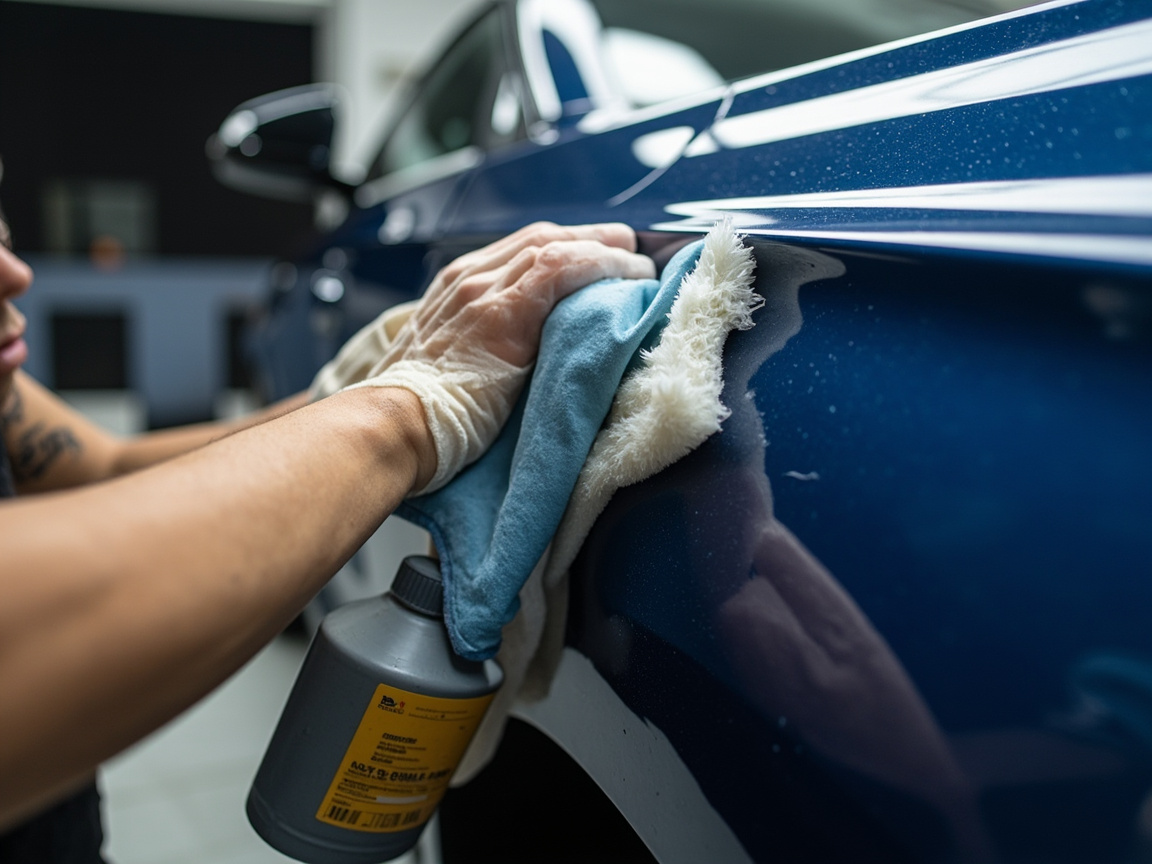
Si-based automotive ceramic coatings widely adopt the process of "small amount multiple times, cross-coating, immediate wiping clean" (per Gaamp360 flow: IPA degreasing → small amount multiple times cross-coating → flash dry 30 s–3 min → wipe clean → avoid water 24–48 h). The core is: use a small cloth pad dipped in minimal coating liquid, cross-coat thinly on the paint surface, let solvent flash dry to form the initial layer, then wipe off excess with a new cloth. Excess material not wiped off will turn white and leave marks after drying.
3.3 Dip Coating / Flow Coating: Preferred for Electronics and Complex Parts
For complex geometries such as PCBs, connectors, and tiny parts, spraying is hard to fully cover, and dip coating or flow coating is more reliable. The electronic superhydrophobic insulating nano ceramic coating ECS 1300AG uses "spraying / wiping / dip coating" multiple methods, and is mainly single-coat (per ECS 1300AG data). The key to dip coating is pull-up speed and dripping control to avoid pooling.
3.4 Film Thickness Control: Awareness of nm to µm Scale
Nano coatings for different uses vary greatly in film thickness and must be controlled per product TDS:
| Coating Type | Typical Film Thickness | Data Source |
|---|---|---|
| Automotive paint nano ceramic shield (Si-based) | 200–400 nm | Onyx Nano Shield |
| Automotive paint ceramic coating (SiO₂-based) | 1–3 µm | Gaamp360 |
| Electronic superhydrophobic insulating coating (aerogel+ceramic) | 12–25 µm | ECS 1300AG |
| Hydrophobic self-cleaning nano composite ceramic coating | 50–100 µm | YC-8703 |
Film thickness should be measured with a step profiler, ellipsometer, or SEM cross-section (nanoscale), not a ordinary wet film comb—the error of ordinary tools would be larger than the film thickness itself.
3.5 Flash Dry and Intercoat
After each coat, a flash dry time is needed for solvent evaporation and network formation to begin. Gaamp360's flash dry window is 30 s–3 min, then wipe clean. When stacking multiple layers, intercoat must also be controlled: too fast and solvent hasn't escaped causing bubbles, too late and the surface has hardened forming a weak interlayer interface.
IV. Curing Window: Temperature, Humidity, and Curing Time
"Applying" a nano coating and "forming the film" are two different things. If the curing window is missed, only half the performance can be achieved.
4.1 Temperature and Humidity Window
Most solvent-based nano ceramic coatings are sensitive to temperature and humidity:
- Gaamp360: Application temperature 5–30°C, relative humidity < 70% (per its TDS);
- General environment for epoxy-polyurethane topcoat types: temperature 5–35°C, relative humidity ≤ 80%, substrate temperature at least 3°C above dew point (per domestic product parameters);
- Minimum application temperature for epoxy types is commonly 10°C (low-temperature dedicated low-temperature curing type required for low temps).
Excessively high humidity not only brings the risk of condensation, but also slows solvent evaporation and induces blushing.
4.2 Initial Curing and Final Curing Are Not the Same
Nano ceramic coatings typically "first surface-dry to form a film, then slowly densify the network":
- Onyx Nano Shield: Initial curing by IR heat treatment for 1 h or at room temperature for 2–3 h; final curing requires 14 days (per its documentation).
- Gaamp360: Initial curing 24–48 h, full curing 5–7 days; heat resistance up to 600°C (per its TDS).
- YC-8703: Touch dry 2 h, hard dry 24 h, ceramization in 7 days; can be fast-cured by baking at 150°C for 30 min (per its TDS).
This means: measuring contact angle immediately after coating, or putting into vehicle service right away, will not yield the final performance. Acceptance should be conducted after final curing.
4.3 Water-Avoidance / Dust-Avoidance Window
Water will damage the incompletely cured inorganic network, causing blushing and reduced adhesion. Gaamp360 explicitly requires water avoidance for 24–48 h; automotive ceramic coating application typically advises no automatic car washing and no waxing within one week. Dust is similar—the uncured wet film will trap dust and form permanent defects.
4.4 Curing Kinetics: Solvent Evaporation + Network Formation
Taking SiO₂ sol-gel type ceramic coating as an example, curing occurs in two steps: the solvent (carrier) evaporates causing the liquid film to shrink and adhere; subsequently siloxane hydrolysis-condensation forms a —Si—O—Si— inorganic network, and hardness and chemical resistance increase accordingly. The higher the temperature and the more suitable the humidity, the faster the condensation, but the final network integrity is still constrained by the total curing time. This is also why "bake fast-cure" can shorten the construction period, yet cannot replace sufficient curing duration.
V. Two Typical Application Process Examples
Example A: Automotive Paint Surface SiO₂ Ceramic Coating (refer to Gaamp360 process)
- Wash car to remove floating dust → IPA degrease twice, ensure no water droplets remain.
- Small cloth pad dipped with minimal coating liquid, apply thin cross-coat by zones.
- Flash dry 30 s–3 min, immediately wipe off excess material with a new cloth.
- Avoid water for 24–48 h, no car wash or waxing within 7 days.
- Accept contact angle and gloss after final curing of 5–7 days.
Example B: Industrial Metal Part Hydrophobic Nano Composite Ceramic Coating (refer to YC-8703 process)
- Sandblast to above Sa 2.5 (46-mesh white corundum), roughness meets standard, oil-free and dust-free.
- Confirm substrate temperature at least 3°C above dew point, relative humidity ≤ 80%.
- Spray film thickness 50–100 µm, evenly covered.
- Touch dry 2 h, hard dry 24 h; if fast cure needed, bake at 150°C for 30 min.
- After 7 days curing to complete ceramization, conduct salt spray and adhesion acceptance.
VI. Acceptance and Testing: Use Data, Not Feel
Nano coatings cannot be judged as "good if it looks shiny"; they should be accepted by the following hard indicators (methods cited from general coating standards):
| Indicator | Recommended Standard | Key Judgment Points |
|---|---|---|
| Contact angle / Roll-off angle | Contact angle meter; self-cleaning refer to ISO 27448 | Superhydrophobic typically > 100°, smaller roll-off angle means better self-cleaning |
| Pencil hardness | GB/T 6739 / ISO 15184 | "9H" must be noted as pencil hardness and depends on substrate |
| Adhesion (cross-cut) | GB/T 9286 / ISO 2409 | Grade 0–1 is excellent (flaking ≤ 5%) |
| Salt spray resistance | GB/T 1771 / ASTM B117 | Judge per grade and TDS (e.g. ≥1200 h) |
| Abrasion (Taber) | GB/T 1768 / ASTM D4060 | Lower weight loss is better |
| Film thickness | Profilometer / Ellipsometry / SEM cross-section | Must fall within TDS specified magnitude |
For testing details and instrument principles, further refer to Detection and Characterization of Nano Coatings: Particle Size, Zeta, Film Thickness and Hardness; for film-forming curing mechanisms, read further Nano Coating Film Formation and Curing: Room Temperature / IR / Baking and Thickness (nm–µm).
VII. Common Application Defects and Troubleshooting
| Defect | High-incidence Stage | Main Cause | Countermeasure |
|---|---|---|---|
| Whole-sheet flaking | Surface treatment | Incomplete degreasing / dew point not controlled | Redo IPA degreasing, measure dew point +3°C |
| Blushing / haze | Curing | High humidity or water contact before curing | Control humidity < 70%, no water within avoidance window |
| Sagging / pooling | Coating | Single heavy coat / incomplete wiping | Thin multiple coats, wipe off excess immediately |
| Poor adhesion | Substrate | Stainless steel not activated / insufficient roughness | Abrade with non-metallic abrasive, sandblast to Sa 2.5 |
| Reduced performance | Acceptance | Tested before final curing | Wait full curing period (e.g. 7–14 days) then test |
| Bubbling | Spraying | Solvent not escaped / substrate contains water | Control moisture, allow sufficient flash-off and intercoat |
Sandblasting and roughness control for industrial parts are consistent with the pretreatment principles of industrial protective coatings; for deeper specifications see Industrial Coating Surface Treatment: Sandblasting Sa2.5, Roughness and Dew Point Control.
VIII. Process Compatibility with Kexin New Materials
Kexin New Materials (kexinMaterials) typically delivers nano ceramic and hydrophobic protective coatings as a package of "pretreatment agent + coating + process card", rather than just selling a bucket of material. The reason lies exactly in what was described above—the success of nano coatings is 70% in the process. For the three scenarios of automotive beauty, electronic protection and industrial anti-corrosion, we separately provide process cards for degreasing formula, sandblasting grade, coating method and curing window, along with third-party testable and verifiable contact angle, adhesion and salt spray data, so that the applicator receives a "directly executable SOP" rather than "parameters to figure out by themselves". This is also the original intention of writing mechanism articles such as Nano Coating Film Formation and Curing into our technical documentation: only by understanding the curing window can performance be stably reproduced.
FAQ
Q: Must sandblasting be done before nano coating application?
A: Not necessarily. Automotive paint surfaces, glass, and cured plastic parts mostly only need IPA degreasing + light polishing; but metal substrates (especially steel, stainless steel) usually require sandblasting to Sa 2.5 (ISO 8501-1) to obtain mechanical anchoring and activated surface. Whether to sandblast depends on substrate type and coating TDS requirements.
Q: Why must the "excess material be wiped off" for nano ceramic coatings?
A: Because such SiO₂ sol-type coatings function via an extremely thin uniform layer; excess material left on the surface will not self-level, and after drying will blanch, leave marks, and even affect hardness uniformity. Processes like Gaamp360 emphasize "small amount multiple times + wipe off after flash dry".
Q: What are the consequences of high application environment humidity?
A: High humidity (e.g. > 70%–80%) may cause substrate condensation (when below dew point by 3°C), and also slows solvent evaporation, inducing film blushing and reduced adhesion. Most nano ceramic coatings require relative humidity < 70% and substrate temperature at least 3°C above dew point.
Q: How long after coating can I wash the car or contact water?
A: Referring to Gaamp360 process, water avoidance for 24–48 h after application is required; automotive ceramic coatings typically advise no automatic car washing within one week. Even if the surface is already touch-dry, final densification of the inorganic network still takes several days.
Q: A nano coating is rated 9H, is it harder than steel?
A: No. "9H" refers to pencil hardness (GB/T 6739), which measures the scratch resistance of the paint film, and the result is affected by substrate support; the nano ceramic layer itself is only nm–µm scale, and its hardness largely comes from the underlying automotive coating/metal substrate. It is "resistant to fine scratches", not "impact-proof or deep-scratch-proof".
Q: Is thicker film thickness always better?
A: For nano coatings, the opposite is true. Too thick tends to sag, crack, and create high stress, and most functionality comes from surface chemistry rather than thickness. Control according to TDS: ceramic layer on automotive coating is often only 1–3 µm, electronic insulating coating 12–25 µm, industrial composite ceramic can reach 50–100 µm.
Q: Can a ordinary wet film comb be used to measure nano coating thickness?
A: Not recommended. Nano layers are only a few hundred nm to a few µm, and the resolution of ordinary wet film combs is far from sufficient. A step profiler, ellipsometer, or SEM cross-section measurement should be used to reflect the true film thickness.
Q: Why should acceptance be after "final curing"?
A: Because initial curing only forms a surface-dry film; the condensation densification of the inorganic network (e.g., —Si—O—Si—) takes time: Onyx needs 14 days, Gaamp360 needs 5–7 days, YC-8703 needs 7 days for ceramicization. Measuring contact angle and hardness before the window will underestimate the true performance.
Q: What if the nano coating on stainless steel easily falls off?
A: Stainless steel surface is dense and inert, and direct coating has poor adhesion. According to TDS, use non-metallic abrasive to sand and create scratches, if necessary do passivation/conversion coating activation, and confirm thorough degreasing. Do not just do ordinary cleaning and then coat.
Q: If the curing temperature is low, will curing be very slow?
A: Yes. The lower the temperature, the slower the solvent evaporation and network condensation. Epoxy types commonly have a minimum application temperature of 10°C, and solvent-based nano ceramic is also mostly above 5°C. At low temperature, low-temperature curing type can be selected, or use 150°C baking for 30 min (e.g., YC-8703) for fast curing, but still need sufficient curing duration.
Further Reading
- Nano Coating Film Formation and Curing: Room Temperature/IR/Baking and Thickness (nm–µm): Explains the film formation and curing dynamics behind the "curing window" in this article, helping to understand why 7–14 days of final curing is needed.
- Nano Coating Wear and Hardness Testing: Pencil Hardness, Taber and Scratch: Details the true meaning and standard basis of "9H", Taber and scratch hardness, to be used with the acceptance section of this article.
- Industrial Coating Surface Preparation: Sandblasting Sa2.5, Roughness and Dew Point Control: General specifications for pretreatment of industrial metal parts, fully consistent with the sandblasting and dew point control principles of nano coatings.