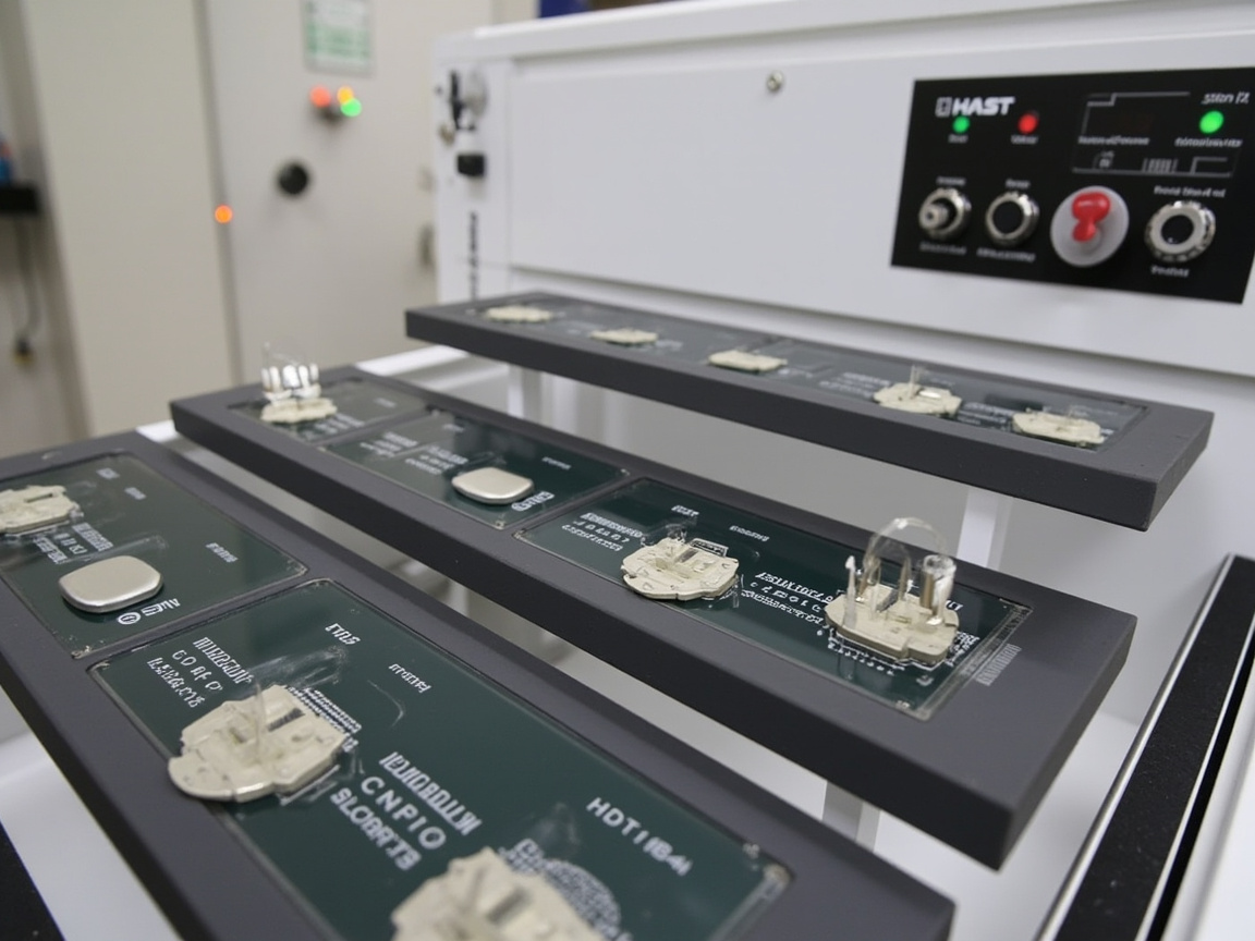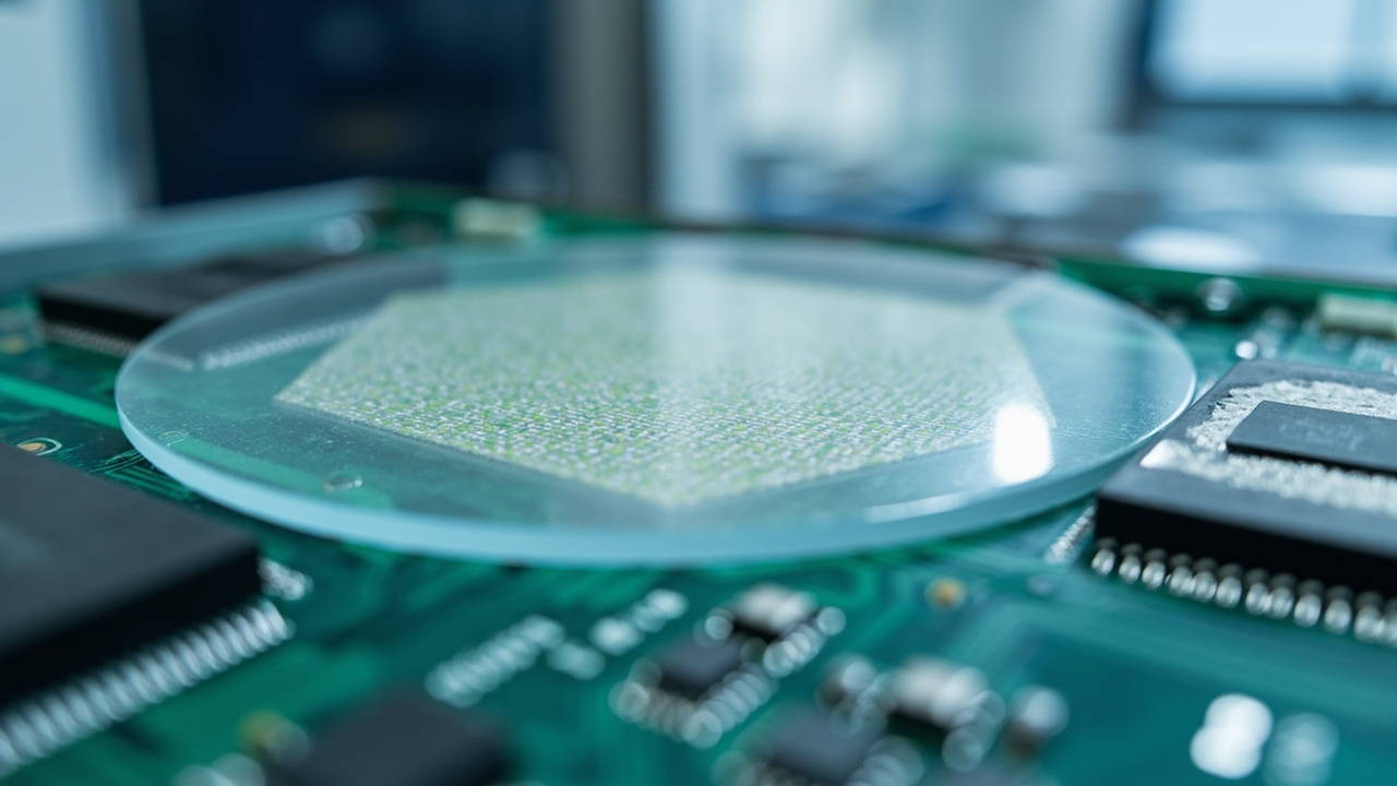
The reliability of semiconductor devices depends to a large extent on the protection of the "last micron." From wafer to package, and from package to board level, chips must face moisture, ionic contamination, thermal cycling stress, mechanical shock, and electromigration. Semiconductor packaging and chip-level protective coatings put an "invisible armor" on these precision structures: providing stress buffering and passivation on the package surface, offering conformal protection at the board level (moisture-proof, salt-spray-proof, mold-proof), and delivering thermal-conductive insulation on power devices. This article clarifies the system, process, verification, and selection of such high-reliability functional coatings, helping electronics and materials engineers establish a framework.
Kexin New Materials (Guangdong) Co., Ltd. has technical reserves in functional protective coatings; its high-reliability conformal and thermally conductive insulating systems can be extended to semiconductor packaging auxiliary protection and power module protection scenarios. Relying on the continuous coating and curing capabilities of its Foshan production base, Kexin New Materials can provide electronic packaging customers with supporting services from material selection to process verification.
I. Overview of Semiconductor Packaging: Protection Layers from Wafer to System
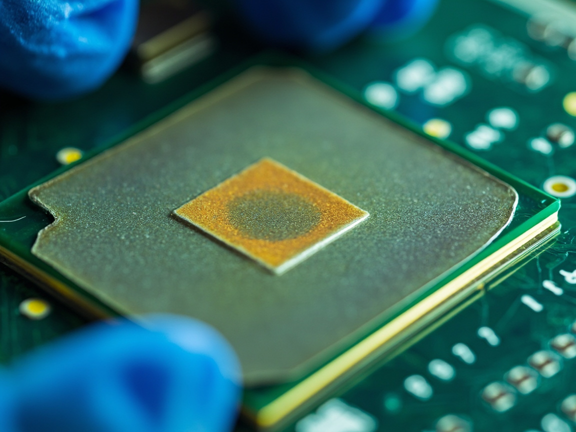
Semiconductor packaging is an engineering discipline that integrates electrical interconnection, mechanical support, environmental protection, and heat dissipation for bare chips (die). Packaging forms have evolved from traditional DIP, SOP, QFP to BGA, CSP, Flip-Chip, SiP, Fan-out Wafer-Level Packaging (FOWLP), and the recently emerging Chiplet multi-die integration. Whether it is a bare die cut from a wafer or a packaged body completed with wire bonding or flip-chip soldering, its metal interconnections, low-dielectric media, solder balls, and bond wires are long-term exposed to moisture, salt, chemical vapors, temperature cycling, and mechanical vibration in the working environment. The inherent duty of packaging is to "protect the chip," and protective coatings are an extension and reinforcement of the packaging's protection capability. At the wafer level, the passivation layer and polyimide/polybenzoxazole redistribution protection layer provide the first line of defense; at the package level, molding compound (EMC), underfill, and surface conformal coating constitute the second line of defense; at the board level, conformal coating forms the third line of defense. The three work in synergy to jointly determine the failure rate of the chip over a service life of ten years or even longer. Understanding the packaging hierarchy is the prerequisite for understanding the positioning of protective coatings: coatings do not replace packaging, but provide additional functional buffering and isolation above, within, and below the packaging. It is worth mentioning that packaging forms are evolving from single-chip to system-in-package (SiP) and multi-die (Chiplet), and the increased interconnection levels make every interface layer a potential entry point for moisture and stress, so the coverage breadth and consistency of protective coatings are thus increasingly important. For materials engineers, the basic method to avoid reliability blind spots is to first map the hierarchical topology of "chip—media—metal—substrate—board level," and then match coating functions and specifications layer by layer.
II. Why Chips Need Protective Coatings: Five Major Failure Mechanisms
Chips are getting smaller and more integrated, and the interconnection density and electric field strength per unit area rise accordingly, amplifying their sensitivity to the environment. The necessity of protective coatings stems from five clear categories of failure mechanisms. The first is moisture intrusion and metal corrosion: aluminum pads and copper interconnections undergo electrochemical corrosion in humid oxygen environments, forming open circuits or leakage. The second is ionic migration and conductive filament (CIIM): under the combined action of electric field and moisture, metal ions migrate along the medium to form dendritic short circuits, which is one of the most hidden and dangerous failures. The third is thermal cycling stress and mechanical cracking: the coefficient of thermal expansion (CTE) mismatch between packaging materials and the chip or substrate generates cumulative stress during temperature cycling, causing cracks in brittle dielectric layers or molding compounds. The fourth is the "popcorn" effect: after the molding compound absorbs water, the vapor pressure rises sharply under the high temperature of reflow soldering, leading to internal delamination of the package. The fifth is alpha particle and soft error: single-event upset caused by trace radioactive isotopes in packaging materials or external radiation. Protective coatings systematically suppress the above mechanisms by isolating moisture and oxygen, passivating surfaces, buffering stress, and reducing ionic mobility. In addition, residual acidic gases inside the package (such as organic acids volatilized from PCB boards) also catalyze corrosion; coatings with low outgassing and low extractable ions can weaken this pathway. It is worth emphasizing that these five mechanisms are not isolated: moisture is often the "accomplice" of both corrosion and ionic migration, and stress cracking opens moisture channels to form positive feedback, so protective design must achieve systematic joint suppression rather than blocking a single gap. Precisely because the mechanisms are complex, semiconductor-grade protective coatings have far higher requirements for purity, stress, dielectric properties, adhesion, and reliability than ordinary industrial coatings.
III. Three Functional Levels of Protective Coatings
According to the location of action, semiconductor protective coatings can be divided into three levels, with significantly different standards and material systems at each level. Wafer-level conformal coating is directly applied on top of the bare die or redistribution layer, requiring extremely low ionic purity, extremely low stress, and low dielectric constant; polyimide (PI), polybenzoxazole (PBO), or spin-on dielectric are commonly used; this is the highest technical threshold layer. Package-level conformal coating acts on the surface or internal voids of completed packages, undertaking stress buffering, underfilling, and moisture-proof passivation; epoxy, silicone, or underfill are commonly used, and it can also be selectively coated on the top surface of the package to form a protective film. Board-level conformal coating is applied on components and solder joints of PCBA to resist moisture, salt, mold, and chemical corrosion; acrylic, polyurethane, silicone, or UV-curable systems are commonly used. The three layers do not replace each other but provide superimposed protection: the wafer level ensures long-term passivation of the chip body, the package level bridges the mechanical and moisture interfaces between chip and substrate, and the board level ensures the survival of the entire assembly in the end-use environment. When doing reliability design, engineers should allocate protection budget according to "which layer is the weakest" rather than applying equal effort.
IV. Overview of Protective Coating Systems: Five Mainstream Types
From a materials chemistry perspective, semiconductor-related protective coatings can be classified into five mainstream types, each suited to different levels and conditions. The first is epoxy, with strong adhesion, good moisture resistance, and controllable cost, widely used for post-molding passivation, underfill, and board-level conformal coating, but with high brittleness and moderate temperature resistance. The second is polyimide (PI) and polybenzoxazole (PBO), with high temperature resistance (long-term withstand above 200℃), low stress, and excellent dielectric properties, being the first choice for wafer-level passivation and redistribution protection layers, but with higher process temperatures (often requiring imidization above 300℃). The third is Parylene, formed by chemical vapor deposition (CVD) into a pinhole-free, ultra-thin, highly consistent conformal coating, suitable for uniform conformal coating of high-reliability, complex 3D morphology devices, but with large equipment investment and higher cost. The fourth is silicone/silicone resin, flexible, temperature-resistant, and low-stress, the preferred choice for power devices and sensor packaging buffering, but with relatively weak moisture resistance, often needing to be combined with a barrier layer. The fifth is solder mask and conformal coating systems (acrylic, polyurethane), mainly serving the board level. The five systems each have trade-offs in purity, stress, thermal conductivity, temperature resistance, and repairability; selection is a trade-off among these dimensions. For ease of engineering selection, the table below gives a comparison of key attributes of the five mainstream protective coatings:
| Type | Max Temp Resistance | Stress Level | Moisture Resistance | Thermal Conductivity | Typical Application Layer |
|---|---|---|---|---|---|
| Epoxy | Medium (~150℃) | Medium—High | Good | Medium | Underfill, board-level conformal coating |
| Polyimide (PI) | High (>300℃) | Low | Excellent | Low | Wafer-level RDL/passivation |
| Polybenzoxazole (PBO) | High (>300℃) | Low | Excellent | Low | High-frequency RDL passivation |
| Parylene | Medium—High | Extremely Low | Excellent | Low | High-reliability conformal coating |
| Silicone/Silicone Resin | High (>200℃) | Extremely Low | Medium | Medium—Low | Power/sensor buffering |
The above table shows typical ranges; specifics are subject to each grade's datasheet; actual selection often uses multilayer composites to complement strengths and weaknesses. In practice, "composite systems" are also common: for example, stacking a layer of Parylene on wafer-level PI to enhance barrier, or coating epoxy over a silicone buffer layer to improve wear resistance, using multiple layers to take the best of each and compensate for the shortcomings of a single material. The differentiated competitiveness of material suppliers often lies not in "whether they have a certain type of resin," but in whether they can turn the multilayer system into a mass-producible, certifiable complete solution for specific packaging structures. This is also the engineering capability most valued by packaging factories when introducing new coatings.
V. Epoxy Packaging Protective Coatings
Epoxy resin is one of the most mature protective materials in semiconductor packaging. Its molecules contain epoxy groups, which cross-link with curing agents (amine, anhydride) to form a three-dimensional network, with extremely strong adhesion to metal, silicon, and glass fiber substrates, relatively controllable water absorption, good dielectric properties, and competitive price. At the package level, epoxy is used for external re-coating of molding compound, lead frame passivation, and underfill; at the board level, epoxy conformal coating provides a tough, chemically resistant moisture-proof layer. The shortcomings of epoxy resin are its high curing shrinkage and brittleness, which easily generate internal stress during large thermal cycles, leading to interface cracking or mismatch with low-CTE materials. For this reason, engineering practices suppress stress by toughening (introducing flexible segments, core-shell rubber particles), reducing modulus, and adjusting curing kinetics. The ionic purity of epoxy depends on raw materials and process cleanliness; semiconductor-grade epoxy must strictly control mobile ions such as Na+, Cl-, K+ to ppm or even ppb levels. Kexin New Materials has accumulated formulation and process experience in epoxy-based high-reliability conformal coatings; its low-stress epoxy system can be used for power module surface protection and board-level moisture-proof scenarios. Specific means of epoxy toughening include introducing core-shell rubber (CSR) particles to absorb crack energy, grafting flexible polyether segments to reduce modulus, and adopting alicyclic epoxy to improve UV and yellowing resistance; these modifications must be finely balanced among toughening, heat resistance, and bonding, otherwise Tg or water absorption will decrease. In engineering, grades are often screened according to the "glass transition temperature—elongation at break—water absorption" ternary diagram, and then closed-loop verified by the above reliability tests.
VI. Polyimide (PI) Coating Materials and Chemistry
Polyimide is the "gold standard" material for wafer-level protection. Its synthesis first polymerizes diamine and dianhydride into polyamic acid (PAA), then undergoes high-temperature imidization dehydration and ring closure to form a rigid aromatic heterocyclic main chain, endowing it with excellent thermal stability (Tg often above 300℃), low dielectric constant (about 3.0–3.5), low dielectric loss, and low moisture absorption. In wafer-level packaging, PI serves as the interlayer dielectric and surface passivation of the redistribution layer (RDL), withstanding multiple photolithography, electroplating, and reflow without failure. The PI coating process is usually spin-coating to form a film, soft baking to remove solvent, high-temperature (250–350℃) imidization, and then photolithography for opening windows. The low stress of PI originates from the flexible ether bonds and moderate cross-linking of its molecular chain, allowing it to buffer the CTE mismatch between chip and metal layers during thermal cycling. The disadvantages are high process temperature, strict requirements on equipment and cleanliness, and the need for precise control of shrinkage during imidization to avoid cracks. Semiconductor-grade PI must also achieve extremely low ionic residue and low outgassing to prevent contamination of sensitive devices.
VII. Polybenzoxazole (PBO) Coating
Polybenzoxazole (PBO) is a protective dielectric that has rapidly gained popularity in advanced packaging after PI. Compared with PI, PBO has a lower dielectric constant (can be below 2.9), lower water absorption (better than PI), higher thermal stability, and better planarization ability, and its imidization (actually cyclodehydration) temperature is slightly lower with a wider process window. In Fan-out wafer-level packaging and 2.5D/3D integration, PBO is often used for RDL passivation and stress buffer layers, especially suitable for ultra-fine line width and multi-layer redistribution scenarios. The low dielectric and low loss characteristics of PBO are particularly critical for high-frequency, high-speed signals (such as 5G, AI chip SerDes channels), reducing signal crosstalk and delay. Its low water absorption further strengthens moisture-proof and anti-ionic-migration capabilities. PBO coating also relies on spin-coating and high-temperature cyclization, with extremely high requirements for film thickness uniformity, pinhole density, and interface adhesion control. Currently, high-end PBO materials are still dominated by foreign capital, but domestic material enterprises are accelerating their catch-up, and Kexin New Materials is also making technical layout in the direction of functional polymer dielectrics.
VIII. Parylene Vapor Deposition Coating
Parylene is a conformal coating formed by vacuum chemical vapor deposition (CVD); its monomer breaks into active dimers in a cracking furnace, then polymerizes on the room-temperature substrate surface, forming a continuous film with uniform thickness (up to hundreds of nanometers to tens of microns), completely pinhole-free, and conforming to complex 3D morphologies. Parylene C, N, HT and other grades have different temperature resistance, dielectric, and barrier properties. Its greatest advantage is uniformity and conformality—slits, blind holes, and dense pin gaps that are difficult to cover with traditional liquid coating can be completely wrapped by vapor deposition, and the film thickness is precisely controlled by deposition time. In aerospace, medical, and high-reliability military electronics, Parylene is often used for devices with extremely strict requirements for moisture-proof, salt-spray-proof, and insulation. The shortcomings are expensive equipment, slow deposition rate, limited capacity and cost, and limited thermal conductivity and mechanical wear resistance when the film is thin. In engineering, Parylene is often combined with other coatings (such as epoxy underfill) to leverage respective advantages. For mass-produced semiconductor devices, Parylene is more suitable for high-value, small-batch high-reliability scenarios. The Parylene HT grade, modified by aromatization, can increase temperature resistance to above 350℃, suitable for power and automotive-grade environments; besides cost, its disadvantages include limited mechanical wear and impact resistance when the film is extremely thin (often < 50μm), and the loading density of the deposition chamber affects capacity. To balance conformality and capacity, a hybrid process of "Parylene + local epoxy reinforcement" has emerged in industry: first vapor-deposit an overall conformal barrier, then spot-coat epoxy on wear-prone areas to increase thickness. Although this mode adds process steps, it can achieve the highest reliability on critical devices with minimal weight gain, and is a typical practice for aerospace and implantable medical electronics.
IX. Silicone and Silicone Resin Flexible Conformal Coating
Silicon-based protective materials use polysiloxane as the main chain, with flexible segments, low glass transition temperature, wide temperature range (-50℃ to above 200℃), and extremely low internal stress, making them ideal for power devices, sensors, and flexible electronic packaging buffering. Silicone conformal coating can effectively absorb thermal cycling and mechanical shock stress, preventing brittle interface cracking; its excellent electrical insulation and weather resistance are also suitable for outdoor and automotive electronics. However, the moisture barrier of pure silicone is weaker than that of epoxy and PI, with a higher water vapor transmission rate (WVTR), so it is often used in combination with a dense barrier layer (such as PI, Parylene, or ceramic fillers). Silicone resin introduces partial cross-linking to improve hardness and adhesion, balancing flexibility and wear resistance. In power modules, silicone is often used for the stress buffer gel on the chip top surface and potting of the housing, absorbing the volume changes brought by SiC device high-temperature cycling. It should be noted that silicone oil migration may contaminate the bonding area; semiconductor-grade silicone must strictly control low volatility and low outgassing.
X. Acrylic and Polyurethane Conformal Coatings
Board-level conformal coating is the most widely used category of protective coatings. Acrylic conformal coating is based on acrylate resin, fast-drying, single-component, soluble in solvent, easy to repair (peelable and re-coatable), and is the mainstream choice for consumer electronics and general PCBA, with balanced moisture-proof, salt-spray-proof, and mold-proof performance, but limited temperature and chemical resistance (long-term operating temperature mostly below 125℃). Polyurethane conformal coating is based on polyurethane resin, with better wear resistance, weather resistance, and chemical corrosion resistance, making it the first choice for outdoor, industrial, and automotive board levels, but some varieties are more difficult to repair and sensitive to humidity. Both can be applied by spraying, dipping, brushing, or selective valve spraying, with film thickness usually controlled at 25–75 microns. In semiconductor board-level assembly (such as sensor modules, power driver boards), conformal coating is the last economical and effective protection barrier. When selecting, trade-offs must be made among repairability, temperature resistance, chemical resistance, and cost, and attention should be paid to its ionic purity to avoid corrosion risks to sensitive solder joints.
XI. Synergy Between Solder Mask and Packaging
Solder mask is a permanent liquid photoimageable coating on the PCB surface; after curing, it forms a green or black insulating protective layer, defining pad openings, preventing bridging, and isolating the direct erosion of copper foil by the external environment. In the board-level protection system, the solder mask is the first and thickest barrier; the conformal coating serves as a superimposed flexible conformal layer, compensating for the solder mask's insufficient coverage of dense gaps and component bodies. Inside the package, a similar idea is reflected in the division of labor between molding compound and surface coating: EMC provides the main mechanical and moisture-proof functions, and the surface conformal coating further passivates and buffers. It is worth noting that the water absorption, ionic residue, and CTE of the solder mask directly affect board-level reliability, especially in lead-free reflow and automotive-grade temperature cycling; therefore, high-end PCBs use low-CTE, low-water-absorption solder mask inks. Incorporating the synergy between solder mask and conformal coating into the overall protection design is the key to improving board-level life.
XII. Low-Dielectric Materials and High-Frequency Signal Integrity
With the popularization of 5G, AI accelerators, and high-speed SerDes, the low-dielectric (low-k) characteristics of packaging and board-level media directly affect signal integrity. Excessive dielectric constant (Dk) and loss factor (Df) cause signal delay, crosstalk, and insertion loss. At the wafer level, PI/PBO are preferred as RDL dielectrics due to their low Dk (about 2.9–3.5); at the board level, high-frequency PCBs use modified epoxy (such as hydrocarbon resin, PTFE composite) to reduce Dk. If the protective coating serves as an additional dielectric on redistribution or component surfaces, it must not significantly raise the equivalent Dk/Df, otherwise it will deteriorate channel performance. Advanced low-dielectric coatings reduce polarization by introducing fluorine groups, porous structures, or aromatic ring regulation, while maintaining sufficient adhesion and moisture resistance. In millimeter-wave and optical module packaging, low-dielectric conformal coating even participates in impedance matching design. Therefore, signal integrity has become a dimension that cannot be ignored in semiconductor protective coating selection, equally important as moisture resistance and stress. The control of loss factor (Df) is also critical: high Df converts into heat and jitter in high-speed channels, especially significantly affecting 112G/224G SerDes and phased-array RF front-ends. Low-Df resins usually rely on low-polarity main chains (such as fluorine-containing, polyolefin, or special aromatic rings), but such structures often have weak adhesion and poor chemical resistance, requiring compensation in interface treatment and curing network. For material enterprises, coatings that can provide "Dk/Df measured frequency-dependent curves" rather than just single-point nominal values are more likely to pass the design review of high-speed packaging.
XIII. Material Purity and Ionic Contamination Control
Purity is the fundamental difference between semiconductor-grade protective coatings and ordinary coatings. Even ppm or even ppb levels of mobile ions such as Na+, Cl-, K+, Br- can trigger metal ionic migration (electromigration / CIIM) under the combined action of bias and moisture, forming conductive dendrites leading to short circuits within hours to thousands of hours. Therefore, the raw materials, solvents, fillers, and processes of semiconductor coatings must be carried out in a clean environment throughout, and the extractable ion content must be determined by internal standard ICP-MS or ion chromatography (IC). The synthesis paths of epoxy, PI, and silicone all need to eliminate halogen catalyst residues, metal impurities, and hydrolysis by-products. At the production line level, operators' sweat, cleaning water, and oven atmosphere can all be pollution sources, which must be guaranteed by ultra-pure water cleaning, clean ovens, and controlled humidity lines. Materials whose ionic purity does not meet specifications (such as total Na+ + Cl- below ppb-level target) must never be used for chip-level conformal coating. Kexin New Materials has established a testing process from raw materials to finished products in the ionic purity control of functional coatings to meet the application threshold of high-reliability electronics. In addition to end-material testing, front-end control also determines success or failure: incoming raw materials must be fully inspected for extractable ions by IC or ICP-MS; solvents must be electronic grade and transported in closed containers; production water must be 18.2 MΩ·cm ultra-pure water; ovens and coating chambers must be regularly cleaned with lint-free cloth and isopropanol and verified for blank residue. Packaging factories will also retest ions and volatiles during incoming quality control (IQC), forming a "supplier—packaging factory" double check; pollution at either end may scrap the entire batch of devices.
XIV. Stress Buffering and Low-Stress Design
Stress is the "invisible killer" of packaging protection. Chips, dielectrics, metals, and substrates have different CTEs, repeatedly expanding and contracting during reflow soldering and service temperature cycles, accumulating shear stress at interfaces; when this exceeds interfacial adhesion or material strength, cracking and delamination occur. Low-stress design runs through both material and process ends: on the material side, resins with low modulus and high elongation at break (such as toughened epoxy, silicone) are used, or flexible segments are introduced into rigid PI; on the structural side, stress concentration is reduced through gradient layers, buffer layers, and arc transitions; on the process side, curing shrinkage is controlled, and stepwise heating and low-temperature post-curing are used to release residual stress. At the wafer level, the intrinsically low-stress properties of PI/PBO allow them to buffer the mismatch between RDL metal layers and the silicon substrate; at the board level, the flexible film of conformal coating absorbs vibration and thermal expansion. Stress can also be predicted in advance through simulation (finite element CTE/modulus modeling), and then optimized via film thickness, fillers, and curing curves. Low stress does not mean softer is better—too soft sacrifices adhesion and wear resistance, and a balance must be struck between buffering and strength.15. Integrated Thermal-Conductive and Insulating Coating (Power Devices)
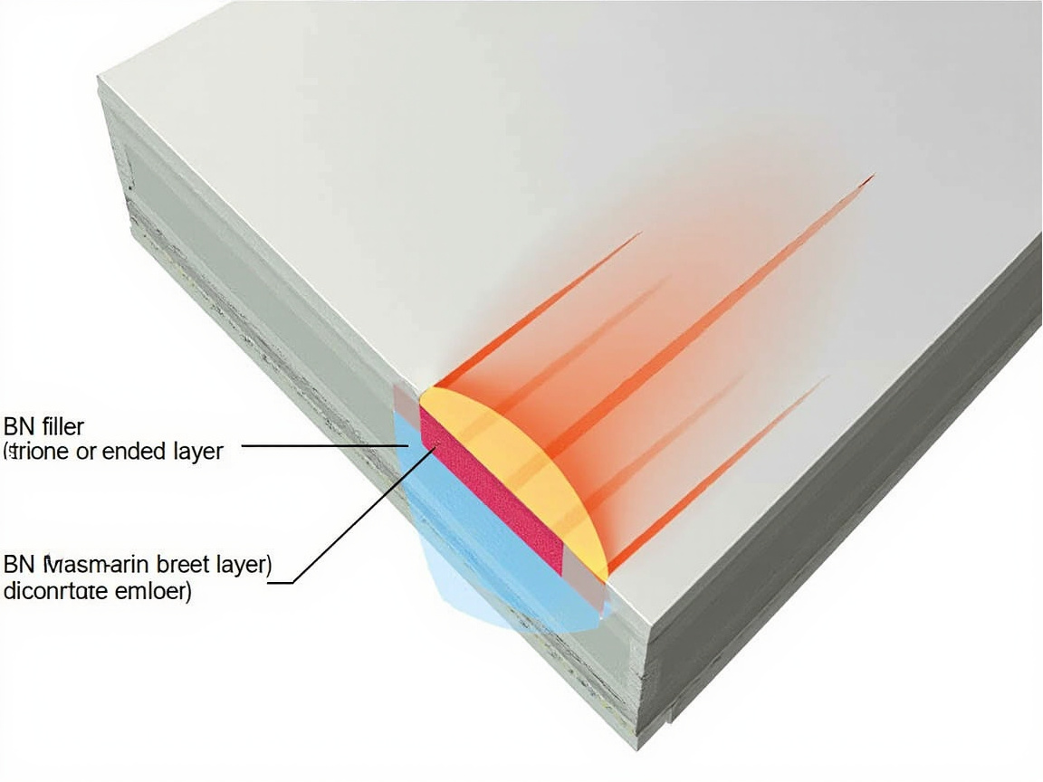
Power devices such as IGBT, SiC, and GaN generate large amounts of heat during operation; for every rise in junction temperature, lifespan declines exponentially; meanwhile, high voltage requires insulation to prevent breakdown. Traditional solutions use ceramic substrates (AMB, DBC) for thermal conduction and insulation, then rely on interfacial materials for connection, but interfacial thermal resistance is large. Thermal-conductive and insulating coating composites insulating resin (epoxy, PI, silicone) with high-thermal-conductive fillers (boron nitride BN, aluminum nitride AlN, alumina Al₂O₃, zinc oxide) to form a thin layer that is both insulating and thermally conductive, directly coated on the top-side of the chip or the inner surface of the module housing, eliminating multiple interfacial layers. The technical difficulty lies in balancing: more fillers and greater orientation (e.g., planar arrangement of flake BN) improve thermal conductivity, but volume resistivity and flexibility drop, and viscosity rises making coating difficult. Engineering approaches use surface-modified fillers, constructing thermal conduction paths (percolation), and controlling filler morphology orientation to approach the triangular optimum of "high thermal conductivity + high insulation + low stress." Kexin New Materials' formulation accumulation in thermal-conductive and insulating coatings can serve the top-side protection of power modules and insulating-thermal conductive coating on inner housings. The orientation mechanism of flake boron nitride (BN) is especially critical: under shear coating or external fields (such as ultrasound, electric field) guidance, BN flakes arrange parallel along the plane, forming an anisotropic channel of "in-plane high thermal conductivity, through-thickness insulation," which both enhances effective thermal conductivity and maintains through-thickness volume resistance. At the same time, filler surfaces modified with silane coupling agents can reduce interfacial thermal resistance, suppress agglomeration, lower the percolation threshold, and reduce filler dosage, thereby preserving resin flexibility and adhesion. The formulation of thermal-conductive and insulating coating is essentially a multi-objective optimization of "filler–interface–resin."
16. Wafer-Level Coating Process
Wafer-level coating uniformly applies PI/PBO/spin-on dielectric on an entire wafer (200mm or 300mm), then undergoes soft bake, exposure, development, and curing to form a patterned protective layer. The core process is spin-coating: liquid resin is dropped on a high-speed rotating wafer, centrifugal force spreads it into a uniform film from sub-micron to several microns, with film thickness adjusted by viscosity and rotation speed; then stepped heating in an oven removes solvent (soft bake), followed by high-temperature imidization or cyclization. The uniformity of spin-coating (film thickness deviation often required < ±5%) directly determines subsequent lithography and electroplating quality, with extremely strict requirements on equipment vibration, environmental cleanliness, and temperature control. Some scenarios use slot-die coating or chemical vapor deposition to accommodate larger areas and thicker films. Wafer-level coating must also control particles, pinholes, and edge bead effects. With the rise of FOWLP and fan-out packaging, wafer-level coating is expanding from mere passivation to RDL dielectric, stress buffering, and redistribution integration, making it one of the core processes of advanced packaging.
17. Panel-Level Packaging (Panel-Level) Coating
Panel-Level Packaging (PLP) transfers wafer-level processes from circular wafers to square panels (e.g., 510×515mm or larger) to reduce unit cost with higher area utilization, and is a key path for Fan-out packaging cost reduction. Panel-level coating faces more complex challenges than wafer-level: greater panel warpage, harder dimensional uniformity control, and different rheological behavior of materials at square corners and edges. Coating methods shift from spin-coating to slot-die coating, spray coating, or roll coating, requiring uniform film thickness, no bubbles, and no orange peel over large areas. Panel-level requires a wider process window for protective coating and is more sensitive to warpage compensation, often needing low-modulus, low-shrinkage materials to suppress panel bending. The proliferation of PLP is driving protective coatings to evolve from "wafer-adapted" to "panel-adapted," posing new challenges for material rheology, curing shrinkage, and adhesion. This is a potential market opportunity for enterprises with continuous coating and formulation development capabilities (such as Kexin New Materials' Foshan production line).
18. Dispensing, Spot Coating, and Underfill (Dam-Fill / Underfill)
Inside packages and at board level, liquid protective materials are often applied via precision dispensing. Underfill is used after Flip-Chip bonding, where epoxy adhesive capillary-flows to fill the tens-of-micron narrow gap between chip and substrate, converting solder ball stress from concentrated to distributed, greatly improving thermal cycle life; capillary underfill (CUF) self-levels by capillary action, while molded underfill (MUF) is filled synchronously during molding. Dam-Fill is used for wafer-level or board-level cavities: first dispense dam gel to define the region, then fill with liquid or paste dielectric, which after curing forms a controlled-thickness protective cavity, commonly used in MEMS, sensors, and power device cavity packaging. Dispensing precision (needle, pressure, trajectory, dispensing volume) directly determines fill completeness and void rate, and is core to yield. On the material side, viscosity, thixotropy, curing rate, and CTE must be adjusted to match the process. Dispensing and underfill are bridge technologies connecting "coating" and "package structure."
19. Process Parameters: Thickness (µm) and Curing Temperature
The performance of protective coating is precisely defined by film thickness and curing curve. Wafer-level PI/PBO dielectric film thickness is mostly 2–15 microns; too thin risks pinholes, too thick raises stress and cost; package-level coating and board-level conformal coating film thickness are mostly in the 25–100 micron range, while power device thermal conductive layers can reach hundreds of microns. Film thickness deviation must be strictly controlled (usually within ±10%), otherwise uneven thickness becomes a weak point for stress and leakage. Curing temperature determines crosslink density and final properties: epoxy thermoset is often 120–180℃, PI imidization requires 250–350℃, silicone addition curing about 150–200℃, and UV conformal coating is room-temperature photocuring supplemented by thermal post-cure. Heating rate, dwell time, and cooling curve affect residual stress and bubbles; improper fast curing locks in solvent forming voids. Determination of process parameters must combine material Tg, CTE, glass transition, and outgassing data, optimized via DOE (Design of Experiments) and closed-loop through reliability verification. Taking underfill as an example, the curing curve must balance "sufficient capillary flow time to fill narrow gaps" and "not pre-locking before gel point," so a two-stage approach is often used: low-temperature pre-cure maintains fluidity, then heating for full crosslinking; film thickness is determined by dispensing volume and gap height, typically 30–80μm. For wafer-level PI, too aggressive imidization heating causes bubbling, too slow hurts throughput, requiring balance between TGA outgassing peak and production tempo. Any parameter change should trigger change control (ECN) and re-sampling for HAST/adhesion verification, ensuring stable and controllable process window.
20. Coating Equipment: Spraying, Selective Coating, and Jet Dispensing
Large-scale application of board-level conformal coating relies on automated coating equipment. Selective coating uses precision valve spraying or Jet dispensing to coat only required protection areas per preset pattern, avoiding connectors, gold fingers, vias, and test points—high precision, material-saving, no hole blockage, and is the mainstream for high-end PCBA mass production. Equipment consists of motion platform (X/Y/Z three-axis or gantry), fluid valve (needle valve, diaphragm valve, screw valve), vision positioning, and curing oven, integrable with UV, hot air, or IR curing. Spray coating suits large-area thin layers but uniformity is inferior to valve spraying; dip coating suits small parts but wastes material and is hard to avoid areas; brush coating is only for repair. Jet dispensing uses piezoelectric or pneumatic jetting for non-contact, high-frequency dispensing, suitable for dense component gaps. Equipment selection must match coating viscosity, film thickness target, and line tempo (UPH), and link with AOI (Automated Optical Inspection) to ensure coverage without omission.
21. Specialized Equipment for Vapor Deposition and Centrifugal Coating
Wafer-level and high-reliability coating rely on dedicated equipment. Spin coater uses vacuum chuck and programmable speed curve for sub-micron uniform film, often integrated with hot plate for soft bake; its cleanliness must reach Class 100 or higher, equipped with particle monitoring. Parylene deposition system consists of evaporator, pyrolysis furnace (about 650–700℃), and deposition chamber, vacuum vapor-phase film formation, with high equipment investment and maintenance cost, but unmatched film quality. Slot-die coater is used for panel-level and thick films, controlling film thickness via precision metering pump and die gap. Common challenges for these equipments are particle control, uniformity, and throughput; semiconductor-grade coating must run in ISO 3–5 micro-environments, with online film thickness (ellipsometer), particle counting, and defect inspection. Equipment investment and process know-how together form industry barriers, and are also the focus for domestic enterprises to break through advanced packaging material support.
22. Quality Control (QC) Overview: Thickness, Adhesion, Leakage, and HAST
QC for semiconductor protective coating is a multi-dimensional, high-sensitivity detection system. Thickness measurement uses profilometer, ellipsometer, or XRF for rapid screening; adhesion uses tape method, cross-cut method, pull-off, and shear testing to evaluate interfacial strength; leakage and insulation use high-resistance meter for volume/surface resistivity, withstand voltage, and leakage current; moisture bias and ion migration use THB, HAST; reliability verification also includes high-low temperature cycling, PCT, and salt spray. Each batch of material must come with ion purity (ICP/IC), thermal analysis (TGA/DSC for Tg), viscosity, and solids content reports. Production line uses SPC (Statistical Process Control) to monitor film thickness, coverage, and defect rate. Any single exceedance may amplify into batch failure at the terminal, so QC is not sample release but full-process closed loop. Kexin New Materials has configured basic capabilities of thickness, adhesion, and insulation in coating inspection, supporting the shipment consistency of its high-reliability coatings. On production lines, Statistical Process Control (SPC) converts film thickness, coverage yield, insulation strength, etc. into control charts (X-bar/R); once trend exceeds control, line stops for tracing; meanwhile batch traceability is established, with full-link archiving from raw material batch number, process parameters to inspection data, meeting automotive and medical customer traceability requirements. For high-reliability coatings, the depth of QC capability directly determines whether they can enter automotive and military supply chains, and is also the basis for long-term trust with packaging factories.
23. Thickness and Uniformity Measurement Technology
Film thickness is the most basic QC indicator for protective coating, with measurement methods varying by film and substrate. Profilometer obtains absolute thickness by probe scanning film edge step, high precision but micro-damaging to sample and low efficiency; ellipsometer uses polarized light phase and amplitude changes at thin-film interface to invert thickness and refractive index, non-contact, suitable for thin layers (nano to micron level), and is the wafer-level PI/PBO online first choice; XRF (X-ray fluorescence) can quickly compare coatings containing specific elements (such as filler metals), suitable for line screening; eddy current and ultrasound are used for thick films. Uniformity includes not only within-wafer deviation, but also wafer-to-wafer and batch-to-batch consistency, usually measured by Cpk. Measurement must avoid edge effects and particle interference, and combine with destructive cross-section (cross-section SEM) for periodic calibration. Once thickness data is abnormal, trace back to coating parameters, viscosity, and curing to form a "measurement–process" closed loop.
24. Adhesion and Bond Strength Testing
Adhesion determines whether the protective layer can "stay attached" long-term under thermal cycling, vibration, and moisture. Common methods include: cross-cut method with tape peel for qualitative assessment; pull-off method using a dolly glued to coating surface to measure interfacial strength with vertical tension, quantifying bond force; shear and peel tests for underfill and adhesives; 90°/180° peel for flexible films. Adhesion is affected by surface energy, roughness, contamination, and curing degree—if substrate retains mold release agent, oxide, or silicone oil, adhesion drops sharply. Semiconductor-grade processes emphasize plasma cleaning, UV ozone treatment to boost surface energy, and strict control of post-treatment dwell time. Adhesion retention after humidity-heat (e.g., after THB) is especially critical, because moisture intrusion most easily starts from interfacial failure. Bond data is core input for material selection and process certification.
25. Ion Migration and Electromigration (CIIM) Testing
Conductive Anodic Filament (CAF) and chip-internal ion migration (CIIM) are the most hidden failure risks for protective coating. Testing typically applies bias on comb pattern specimens placed in high-temperature high-humidity environment (e.g., 85℃/85%RH + bias THB), monitoring insulation resistance decay over time until dendrite short circuit appears. The coating's ion purity, water absorption, barrier property, and interfacial sealing together determine migration time (MTTF). For epoxy, PI, silicone, low ion residue + low WVTR + no pinholes are the three elements to suppress migration. Emerging bias-HAST (high-pressure steam + bias) further accelerates this process, used for automotive and military-grade certification. CIIM test results are the gold standard for verifying "whether the coating truly blocks ion channels," and also the core basis for high-end material premium.
26. Highly Accelerated Stress Test HAST/PCT and THB
Highly Accelerated Stress Test (HAST) and Pressure Cooker Test (PCT, often 121℃ saturated steam at atmospheric pressure) are the "pressure cookers" of semiconductor reliability. HAST at 110–130℃, 85%RH, optionally with bias, compresses years of natural aging into tens to hundreds of hours, rapidly exposing moisture-related failures (corrosion, delamination, migration). THB (Temperature Humidity Bias) at 85℃/85%RH + operating bias accelerates ion migration and leakage. These tests pose extreme challenges to the sealing, purity, and adhesion of protective coating: any pinhole, microcrack, or mobile ion will be exposed in HAST. After testing, appearance, electrical, and cross-section analysis (CSAM, SEM) must be done to confirm failure mode. Passing HAST/THB is the entry threshold for automotive and high-reliability devices, and also key evidence for material enterprises and packaging factories to build trust. Typical HAST conditions are 130℃, 85%RH, bias several to tens of volts, lasting 96–264 hours, with acceleration factor up to thousand-fold of natural environment; PCT often uses 121℃, 2 atm saturated steam to assess package moisture absorption and delamination. It should be noted that accelerated test results are "relative life" not absolute life; engineering must combine Arrhenius and Peck models for extrapolation, and calibrate with field return data to avoid over-interpreting single test duration. Rigorous reliability argumentation is always the cornerstone of protective coating credibility.
27. Common Defects and Countermeasures (Summary Table)
| Defect | Main Cause | Countermeasure |
|---|---|---|
| Delamination/Popcorn | Moisture absorption, high stress, insufficient adhesion | Low-stress material, pre-bake dehumidification, plasma pretreatment |
| Ion migration short circuit | Low purity, humid bias, pinholes | High-purity material, low WVTR, dense film formation |
| Coating bubbles/voids | Process entrainment, moisture cure, solvent lock-in | Control ambient humidity, degassing, stepwise curing |
| Bridging/uneven coverage | Poor coating precision, unsuitable viscosity | Selective coating, adjust viscosity and parameters |
| Cracks/cracking | CTE mismatch, fast cure, brittle | Toughening, gradient layer, slow heating |
| Insufficient thermal conductivity | Low filler, no orientation | Increase filler, promote flake orientation |
| Repair difficulty | Non-strippable coating type | Select repairable conformal coating |
| Particles/pinholes | Insufficient cleanliness | Raise cleanliness class, filtration |
28. Root Cause Analysis of Cracks and Cracking
Coating cracking mostly originates from thermomechanical mismatch and process stress. Chips (silicon CTE≈3ppm/℃) and organic dielectric, substrate (CTE tens to twenties ppm/℃) have vast expansion differences during temperature cycles, accumulating interfacial shear stress; if coating modulus is too high and elongation at break insufficient, cracks initiate at corners, edges, or steps. Fast curing or one-shot thick film locks in solvent and internal stress, cracking after temperature recovery. Filler distribution of molding compound, CTE match of underfill are also critical. Root cause analysis means include CSAM (Scanning Acoustic Microscope) to find internal delamination, dye-penetrant to locate crack channels, FIB-SEM cross-section to observe microcrack morphology, finite element simulation to locate stress concentration. Countermeasures are material toughening (core-shell rubber, flexible segments), structural buffering (arc transition, gradient layer), gentle process (stepwise heating, low-temperature post-cure), and thickness optimization. Cracking is irreversible failure; prevention far outweighs remedy.
29. Void and Delamination Control
Voids and delamination are the most common interfacial defects in packaging protection. Voids refer to gas entrapment inside coating or underfill, or between interfaces (diameter from sub-micron to hundreds of microns), sources include incomplete solvent removal, moisture, air卷入 during dispensing, curing outgassing; delamination refers to loss of adhesion between coating and substrate or between layers. Both become channels for moisture and stress concentration, inducing corrosion and cracking. Control is multi-layered: material side reduces viscosity, adjusts thixotropy and volatiles; process side vacuum degassing, pre-bake dehumidification, optimize dispensing trajectory and curing curve (avoid sudden heating locking gas); equipment side uses vacuum dispensing and online degassing; inspection side uses CSAM, X-ray, and C-SAM scanning to quantify void rate and set upper limit (e.g., < 5% area). Delamination prevention relies on surface plasma cleaning, coupling agent to boost interfacial energy, and low-modulus CTE match. Void/delam rate is the key red line for underfill and thermal conductive layer certification.
30. Application Industries: Logic and Computing Chips
Logic and computing chips (CPU, GPU, SoC, ASIC) demand of protective coating focus on low dielectric, low stress, and high purity. In advanced packaging (Flip-Chip, Fan-out, Chiplet), PI/PBO as RDL dielectric and passivation determines interconnect density and signal integrity; underfill ensures flip-chip solder ball life over thousands of thermal cycles; board-level conformal coating protects AI accelerator card power supply and peripheral components. As compute density soars, packaging thermal management pressure grows, and synergy of thermal interface and insulating coating becomes important. This field is dominated by international material giants, but domestic substitution is accelerating in RDL dielectric, underfill, and conformal coating segments. Although Kexin New Materials mainly targets industrial functional coatings, its low-stress coating and thermal-conductive insulating technology can horizontally support auxiliary protection of computing hardware and power supply module protection. Worth adding is that AI servers' requirements for board-level power and thermal are forcing conformal and thermal materials to upgrade: high-current power modules have concentrated heat, needing both moisture-proof conformal and insulating thermal conduction; traditional "conformal coating + thermal pad" split solution is gradually replaced by "integrated thermal-conductive insulating coating." The computing race is therefore not only in chip process, but also in packaging and board-level material systems; the value of protective coating is shifting from "passive protection" to "actively enabling thermal and reliability."
31. Power Semiconductor and Automotive Electronics (IGBT/SiC)
Power semiconductors (IGBT modules, SiC MOSFET, GaN HEMT) are the fastest-growing field for protective coating demand. Electric vehicles, photovoltaic inverters, charging piles, and energy storage have extremely high requirements for power density and efficiency; the operating junction temperature of SiC/GaN can reach above 175–200℃, far exceeding traditional Si. This requires protective coatings to withstand higher temperatures, higher thermal conductivity and insulation, and low-stress matching of the thermal expansion of wide-bandgap materials; at the same time, modules must guarantee a fifteen-year lifespan in automotive vibration, temperature cycling, and humid environments. Typical applications include thermal-conductive insulating coating on the top surface of chips, insulating coating on the inner wall of housings, conformal coating for busbars and terminals, and underfill reinforcement. Thermal-conductive insulating coatings here both reduce interfacial thermal resistance and prevent creepage, offering outstanding value. Kexin New Materials is located in Foshan—the gathering place of the South China automotive electronics and power device industry chain—and its thermal-conductive insulating and high-reliability coating systems can serve local power module customers nearby. In electric drives and on-board chargers (OBC), power modules frequently endure temperature shocks and mechanical vibrations from start-stop and road conditions; the coating's "low stress + high adhesion" is more decisive for lifespan than mere high thermal conductivity; whereas in battery management systems (BMS) and domain controller board levels, the conformal coating must maintain insulation long-term in the high-temperature, high-humidity, high-salt-spray environment of the engine compartment. Automotive electronics protection therefore presents a dual demand of "module-level thermal-conductive insulation + board-level conformal coating," imposing higher requirements on material enterprises' systematic supply and simultaneous certification capabilities.
32. Automotive IC Reliability Requirements (AEC-Q100)
The AEC-Q100 established by the Automotive Electronics Council is the reliability baseline for automotive-grade chips, imposing systematic requirements on protective coatings: they must pass temperature cycling (e.g., -55℃ to 150℃ for thousands of cycles), high-temperature operating life (HTOL), THB, HAST, solderability, electrostatic discharge (ESD), and other stresses, with a failure rate target at ppm level (zero-defect oriented). This means the coating's purity, sealing, adhesion, and temperature resistance must be maintained under the most severe operating conditions. Automotive standards also emphasize traceability and change control (PCN); any change in material formulation, process, or production line must be re-certified. For protective coating suppliers, entering the automotive-grade supply chain requires establishing an IATF 16949 system and a complete reliability database. This is precisely the moat of high-reliability coating enterprises—Kexin New Materials' systematic capability in functional protection provides a foundation for its extension into automotive electronics auxiliary protection.
33. Environmental Compliance: Halogen-Free and RoHS
Environmental compliance of electronic materials has become a mandatory threshold. RoHS restricts hazardous substances such as lead, cadmium, mercury; REACH controls chemical registration; and "halogen-free" requires the total amount of halogens such as Br and Cl to be below limits (e.g., Cl+Br < 1500ppm) to prevent dioxin generation during incineration. Traditional flame retardancy often relies on brominated and antimony synergistic effects; halogen-free forces materials to shift to phosphorus-based, nitrogen-based, and inorganic hydroxide intumescent flame retardancy. Halogen-free of semiconductor protective coatings requires rebalancing among flame retardancy, insulation, and heat resistance, avoiding the introduction of high dielectric gradients or ionic impurities. Green compliance also extends to low VOC, low outgassing, and recyclable design. Kexin New Materials adheres to halogen-free and low VOC directions in formula development, making its thermal-conductive insulating and conformal coating products meet the environmental requirements of export electronics and automotive customers.
34. Supply Chain and Localization Opportunities (Kexin New Materials Foshan Production Line)
Semiconductor protective coatings have long been dominated by American, Japanese, and European material giants, especially in wafer-level PI/PBO, parylene, and high-end underfill. In recent years, driven by both geopolitics and cost, domestic substitution has accelerated: from EMC, underfill to board-level conformal coating, local enterprises are gradually entering. The Pearl River Delta, as a global electronics manufacturing and packaging hub, has an urgent need for high-reliability, low-cost, and fast-responsive localized materials. Relying on its Foshan production base, Kexin New Materials (kexinMaterials) possesses capabilities in formula development of functional protective coatings, continuous coating and curing processes, as well as ionic purity and insulation thermal conductivity testing. Its product matrix covers epoxy coating, thermal-conductive insulation, conformal coating, etc., providing domestic options in scenarios such as power module protection, board-level moisture-proofing, and industrial electronic packaging auxiliary protection. For packaging factories and OEMs, cultivating a diversified, localized coating supply chain is a strategic choice for cost reduction and supply assurance. Localization also brings response speed advantages: formula fine-tuning, small-batch trial production, and failure collaborative analysis can be closed within a one-day drive, far superior to the cycle of transoceanic supply. Centered on Foshan, the Pearl River Delta gathers a complete chain from packaging and testing, power modules to terminal OEMs. Kexin New Materials (kexinMaterials) can rely on geographic and engineering proximity to provide "material + process" joint development services, helping customers shorten certification cycles when introducing new coatings. Against the backdrop of geopolitical disturbances and supply uncertainty, such nearshore, verifiable, and iterable supply relationships are becoming the core resilience assets of electronics manufacturing enterprises.
35. Standards and Specifications (IPC / JEDEC / MIL)
The selection and certification of semiconductor protective coatings must benchmark against authoritative standards. The IPC series (e.g., IPC-CC-830 conformal coating, IPC-A-610 acceptability) defines the performance and appearance requirements of board-level coatings; JEDEC (e.g., J-STD-020 moisture sensitivity, JESD22 series humidity-temperature bias/cycling) specifies chip-level reliability tests; IEC and UL provide insulation, flame retardancy, and safety regulations; MIL standards (e.g., MIL-I-46058C, being replaced by IPC) remain a reference for military high reliability; automotive looks at AEC-Q series and IATF 16949. Material datasheets must provide comparable data of Tg, CTE, dielectric, WVTR, ionic purity, dielectric strength, and reliability using the methods of these standards. When comparing across suppliers, engineers should base on measured data under the same standard, not marketing claims. Adherence to standards is the bridge for protective coatings from "usable" to "trustworthy." Taking board-level conformal coating as an example, IPC-CC-830 clearly distinguishes the electrical, environmental, and durability requirements of Type AR/ER/UR/SR/XY resins, and specifies the minimum criteria for coating integrity, thickness, and adhesion; UL 746E controls the long-term thermal aging and flame retardancy of insulating parts. When establishing internal specifications (such as corporate QPA), packaging factories often combine these general standards with the failure rate targets of specific devices to form executable and auditable acceptance checklists.
36. Trends and Outlook: Chiplet, Advanced Packaging, and Third-Generation Semiconductors
The future of semiconductor protective coatings is driven by three major trends. First, Chiplet and 2.5D/3D integration push interconnect density and thermal density to new highs, requiring RDL dielectric to be thinner, lower dielectric, lower stress, and wafer-level coating evolving toward lithographic definition precision. Second, the proliferation of third-generation semiconductors (SiC/GaN) makes coatings that withstand higher temperatures, higher thermal conductivity and insulation, and low-stress match wide-bandgap materials a rigid demand; integrated thermal-conductive insulation is the main battlefield. Third, green and repairable orientation drives halogen-free, low VOC, peelable eco-friendly conformal coating, as well as material design for circular economy. At the same time, panel-level packaging cost reduction will reshape coating processes and equipment patterns. The threshold of semiconductor protective coatings has always been the trinity of "purity + stress + reliability," which is the technical high ground of material enterprises. Kexin New Materials (kexinMaterials)'s accumulation in functional protection is gradually extending to power module protection and high-reliability coating, expected to occupy a place in the wave of domestic substitution. From a longer cycle, sustainable development will also reshape material routes: water-based, solvent-free, and peelable recyclable coatings can reduce VOC and the difficulty of waste circuit board treatment; exploration of bio-based or low-toxic monomers is still early but represents the industry's environmental responsibility direction. For manufacturing enterprises, grasping the rebalancing of "high performance—compliance—cost" is both a technical challenge and the key to building competitiveness in the domestic substitution window of semiconductor materials. Kexin New Materials will continue to rely on its Foshan production line to steadily migrate the mature capabilities of industrial functional coatings to semiconductor auxiliary protection scenarios.
FAQ
Q1: Are conformal coating and chip-level coating the same thing?
No. Conformal coating is used for board-level PCBA moisture-proofing and salt-spray resistance; chip-level coating is used at wafer/package level, requiring higher purity, lower stress, lower dielectric—their standards and materials are different.
Q2: Should power device coatings be insulating or thermal-conductive?
Both. Power devices require the dual function of "insulation + thermal conduction," achieved by insulating resin filled with thermal conductive fillers; the difficulty lies in balancing the two.
Q3: Why is semiconductor coating so particular about purity?
Trace amounts of Na+, Cl- will ion-migrate and short-circuit under humid bias, and high temperature accelerates it. If purity is not up to standard, reliability tests will surely fail, so ionic purity is a hard indicator.
Q4: Can board-level conformal coating be repaired?
Depends on the coating type. Acrylic conformal coating is mostly soluble and peelable for easy repair; polyurethane/epoxy are partly difficult to repair. Production lines often select coatings based on repairability.
Q5: Why is selective coating the mainstream?
It only coats the areas needing protection, avoiding through-holes/connectors, with high precision, material saving, and no hole blockage, suitable for high-density board mass production, superior to whole-board brushing/spraying.
Q6: What are the new requirements of SiC/GaN for protective coatings?
Higher operating temperature and greater power density require coatings to withstand higher temperature, higher thermal conductivity and insulation, and low-stress match the thermal expansion of wide-bandgap materials, with a higher threshold than traditional Si devices.
Q7: How to choose between wafer-level PI and PBO?
Both are heat-resistant and low-stress; PBO has lower dielectric, smaller water absorption, wider process window, suitable for high-frequency and ultra-fine RDL; PI has better cost and maturity, suitable for general wafer-level passivation. The decision should combine signal rate, number of layers, and production line capability.
Q8: What to do if protective coating delamination occurs?
First root-cause analysis: mostly moisture absorption, stress, or insufficient pre-treatment. Countermeasures include pre-baking dehumidification, low-stress materials, plasma cleaning to improve adhesion, gradient layer buffering; delaminated parts are usually irreparable and must be prevented from design and process.
Q9: Is parylene suitable for large-scale semiconductor mass production?
Parylene has excellent film quality but expensive equipment, slow deposition, high cost, more suitable for high-value, small-batch high-reliability devices; large-scale general protection still mainly uses liquid-phase conformal coating and underfill.
Q10: Will halogen-free coatings affect insulation or flame retardancy?
A reasonably formulated halogen-free system can achieve equivalent flame retardancy through phosphorus/nitrogen/inorganic flame retardants without sacrificing insulation, but requires rebalancing in heat resistance and ionic purity; selection should look at measured UL/RoHS data.
Further Reading
- New Energy Battery Insulation and Thermal Management Coatings — Industrial comparison of high-reliability insulation protection.
- Energy Storage System Fire-Retardant Coatings — Fireproof and thermal insulation supporting for battery systems.
- Plastic Plating Pre- and Post-Treatment Coatings — Pre-treatment comparison for plastic packaging/metalization.